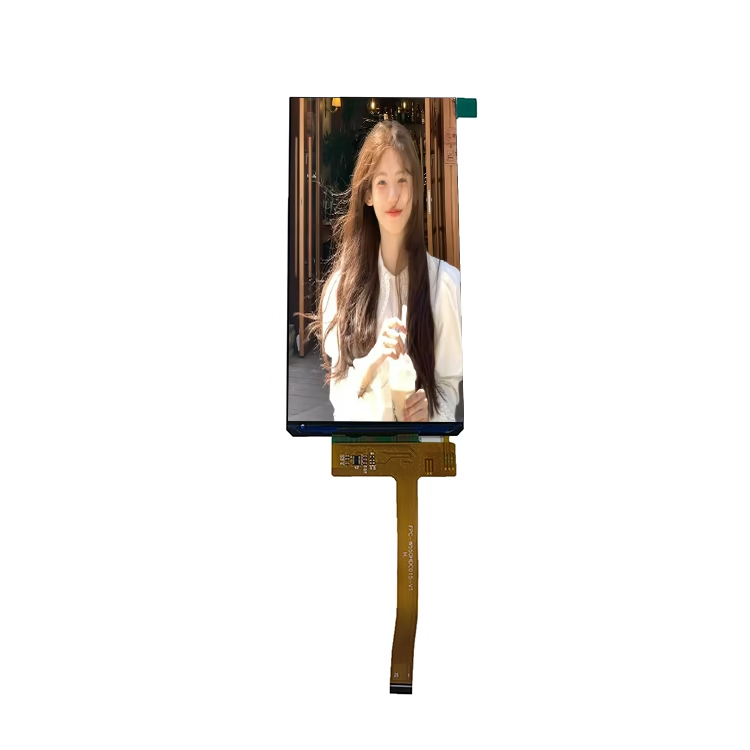
The FPC/Interface/luminance/Touch panel/Cover glass of our most products is customizable.
If you have any requirements, please contact us.
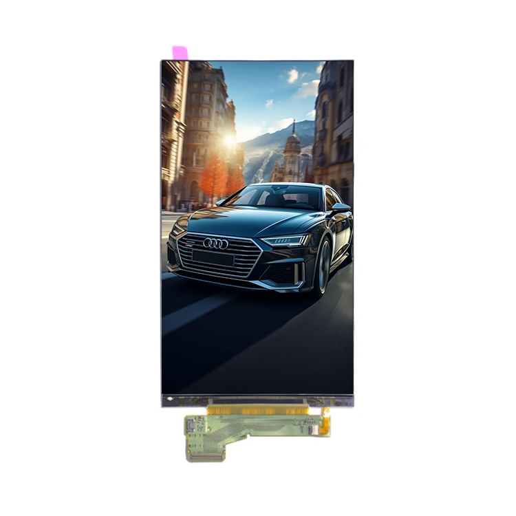
W700WVC013-A is 7 inch TN 6 o’clock viewing angle tft lcd display screen with RGB 24bit interface. Customization is available. The shape is a rectangle with resolution 800*480. Outline dimension is 165x100mm, thickness is 5.7mm. Active area is 154.08×85.92mm. This lcd display is coming out with 50 pins definition. Driver IC is ILI6122+ILI5960, operating voltage is 3.0V~3.6V. Working temperature is -20 to +70℃, storage temperature is -30 to +80℃.
DRAWING

SPECIFICATIONS
| General Specification | |
|---|---|
| Part No. | W700WVC013-A |
| Outline Dimension(mm) | 165 (W)X100(H)X5.7(T) |
| Active Area(mm) | 154.08 (H)X85.92 (V) |
| Number of Pixel(pixels) | 800X(RGB)X480 |
| Touch panel | with or without optional |
| Operating temperature(°C) | -20 ~ +70℃ |
| Storage temperature(°C) | -30 ~ +80℃ |
| Driver IC | ILI6122+ILI5960 |
| Brightness | 1000nits |
| Pixel arrangement | RGB stripe |
| Display mode | Normally white,Transmissive |
| Interface | TTL (RGB-24BIT) |
| Viewing Direction | 6 o'clock |
| Backlight | White LED |
| Module lifetime(Hours) | 50000 |
| Pins Description | ||||
|---|---|---|---|---|
| PIN NO. | Symbol | I/O or connect to | Description | When not in use |
| 1 | GND | PWR SUPPLY | Power ground. | - |
| 2-3 | VDD | PWR SUPPLY | Voltage input pin for internal logic. 2.5V-3.3V. | - |
| 4-5 | LED+ | LED DRIVER | Backlight anode. | - |
| 6 | NC | - | No connect. | - |
| 7 | GND | PWR SUPPLY | Power ground. | - |
| 8-11 | R0-R3 | I/O | Red signal data bus. | GND/IOVCC |
| 12 | GND | PWR SUPPLY | Power ground. | - |
| 13-16 | R4-R7 | I/O | Red signal data bus. | GND/IOVCC |
| 17 | GND | PWR SUPPLY | Power ground. | - |
| 18-21 | G0-G3 | I/O | Green signal data bus. | GND/IOVCC |
| 22 | GND | PWR SUPPLY | Power ground. | - |
| 23-26 | G4-G7 | I/O | Green signal data bus. | GND/IOVCC |
| 27 | GND | I/O | Power ground. | - |
| 28-31 | B0-B3 | I/O | Blue signal data bus. | GND/IOVCC |
| 32 | GND | I/O | Power ground. | - |
| 33-36 | B4-B7 | I/O | Blue signal data bus. | GND/IOVCC |
| 37 | GND | I/O | Power ground. | - |
| 38 | HSYNC | I/O | Horizontal sync input. | GND/IOVCC |
| 39 | VSYNC | I/O | Vertical sync input. | GND/IOVCC |
| 40 | GND | I/O | Power ground. | - |
| 41 | DE | I/O | Data enable signal. | GND/IOVCC |
| 42 | GND | I/O | Power ground. | - |
| 43 | DCLK | I/O | Clock signal in serial. | GND/IOVCC |
| 44 | GND | I/O | Power ground. | - |
| 45 | NC/CS | I/O | No connect/ A chip select signal. | - |
| 46 | NC/SDA | I/O | No connect/ ”L” , this pin act as 3-wire “SDA” pin. | - |
| 47 | NC/SCL | I/O | No connect/ ”L” , this pin act as 3-wire “SCL” pin. | - |
| 48 | DISP | I/O | Standby mode control. “H ”, normal operation. | GND/IOVCC |
| 49 | RESET | I/O | System Reset | - |
| 50 | GND | I/O | Power ground. | - |