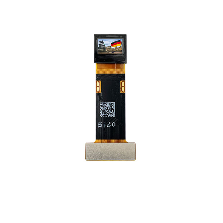
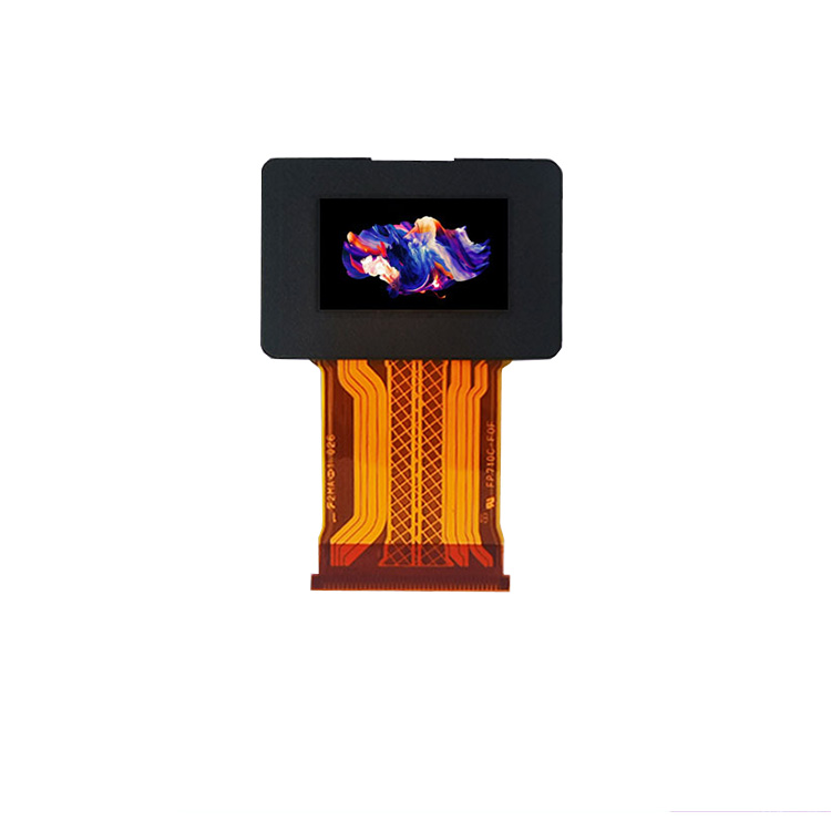
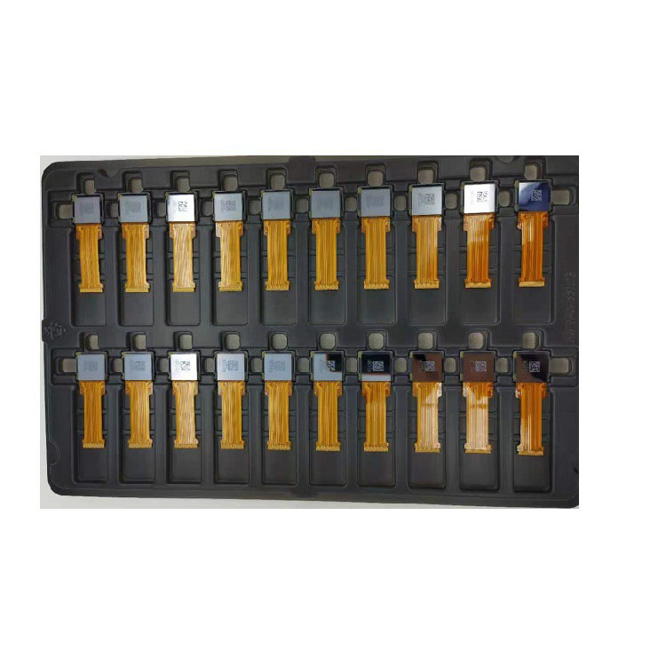
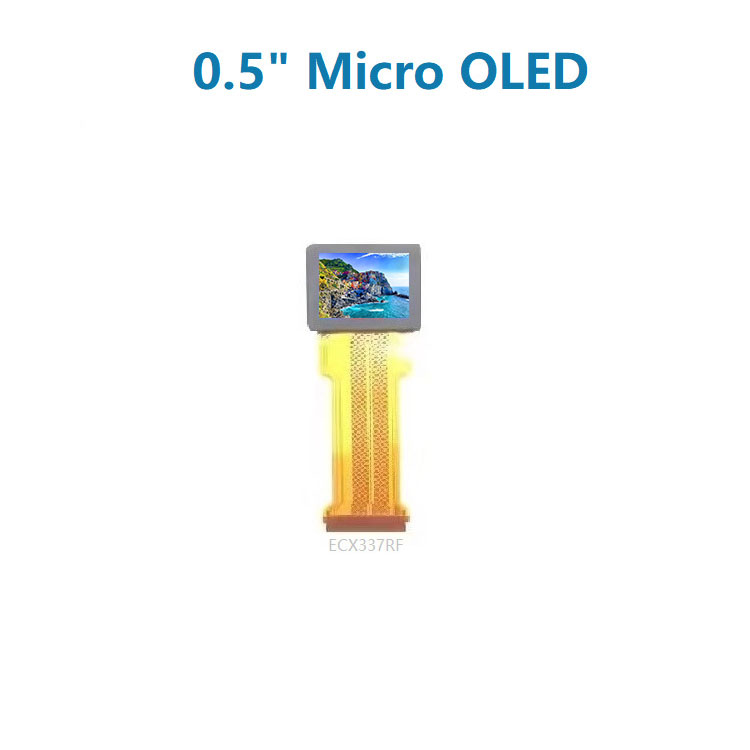
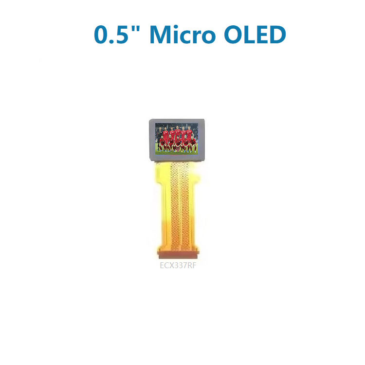
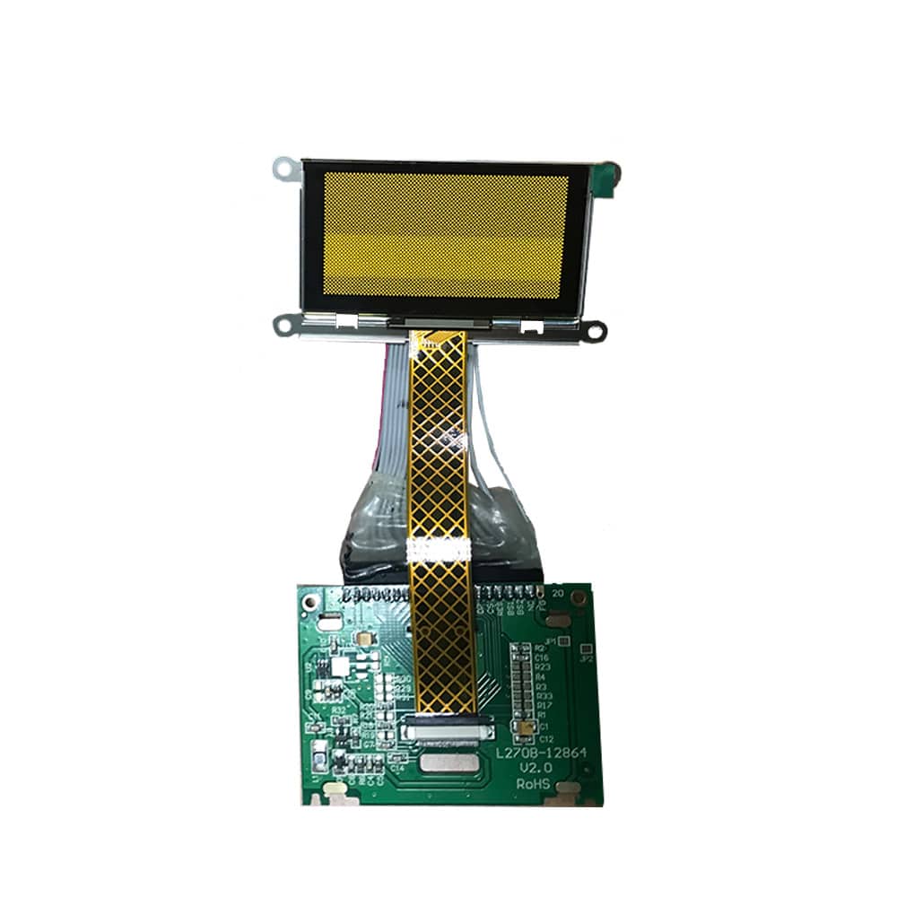
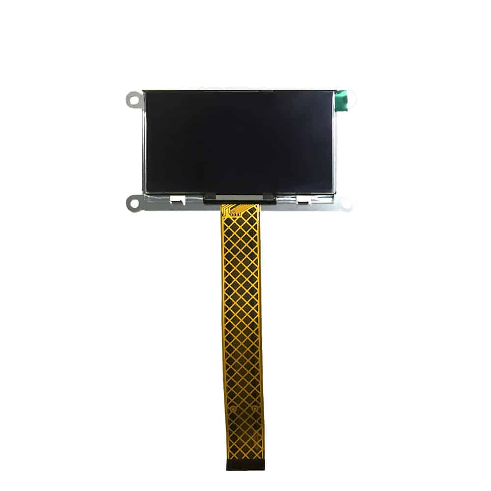
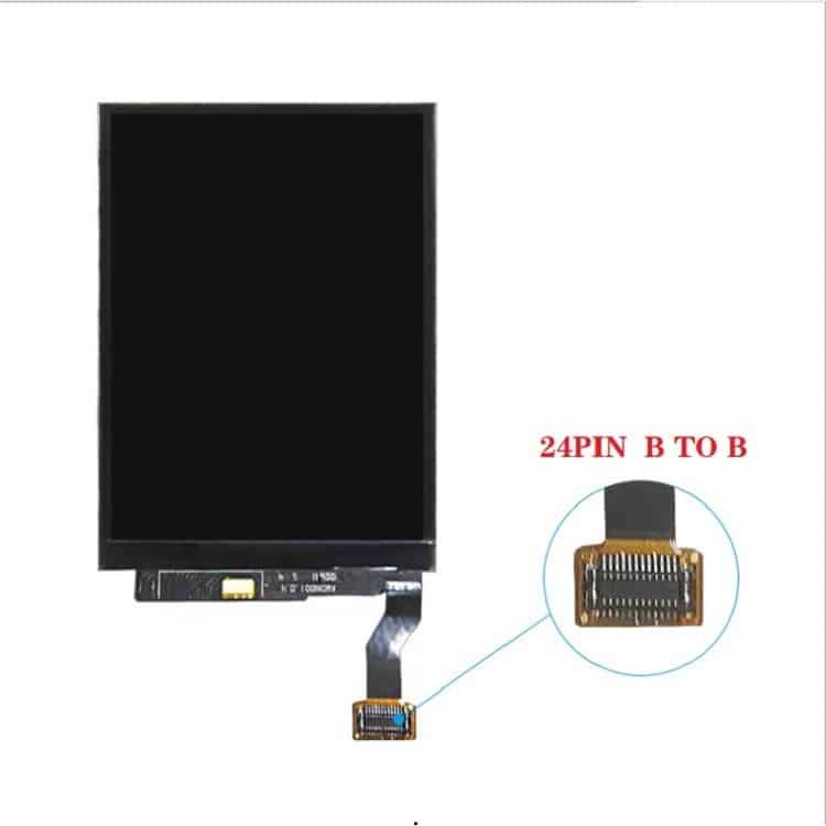
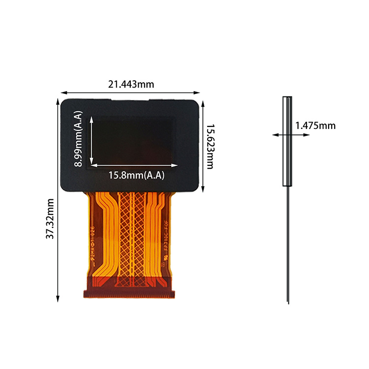
ECX337AF is 0.5 inch mini oled display screen .The shape is a rectangle with resolution 1280*960. Outline dimension is 17.8 x 15.2 mm, thickness is 2.175mm. Active area is 10.14 x 7.644 mm. This oled display is coming out with 61 pins definitions.
DRAWING

SPECIFICATIONS
| General Specification | |
|---|---|
| Part No. | ECX337AF |
| Size | 0.5 inch |
| PCB Outline Dimension(mm) | 17.8(H)x15.2(V)x2.175(T) |
| Active Area(mm) | 10.14 (H)X7.644 (V) |
| Number of Pixel(pixels) | 1280(RGB)*960 |
| Display Type | AMOLED |
| Luminance | 1000nits |
| Contrast Ratio | 10000:1 |
| Operating temperature(°C) | -10 ~ +70℃ |
| Storage temperature(°C) | -30 ~ +80℃ |
| Pins Description | ||||
|---|---|---|---|---|
| Pin No.(FPC Side) | Symbol | I/O Type | Voltage System | Description |
| 1 | VCATH | GND(0) | 10V | EL Cathode Voltage (Connect to GND) |
| 2 | VCCP_O | Power Output | 10V | LDO Output |
| 3 | VDD2 | Power Input | 10V | VDD2 Power Supply |
| 4 | VSS | GND | 10V | Ground |
| 5 | VDD1 | Power Input | 1.8V | VDD1 Power Supply |
| 6 | TEST | Power Input | 10V | Test Pin (Connect to GND) |
| 7 | TEST | Input | 1.8V | Test Pin (Connect to GND) |
| 8 | xCS | Input | 1.8V | SPI Communication Chip Select |
| 9 | XSCK | Input | 1.8V | SPI Communication Clock |
| 10 | SI | Input | 1.8V | SPI Communication Data Input |
| 11 | So | Output | 1.8V | SPI Communication Data Output |
| 12 | TEST | Output | 1.8V | Test Pin (Open) |
| 13 | TEST | Input | 1.8V | Test Pin (Connect to GND)) |
| 14 | TEST | Input | 1.8V | Test Pin (Connect to VDD1) |
| 15 | XCLR | Input | 1.8V | System Reset Signal |
| 16 | VSSIF | GND | 1.8V | Interface GND※ |
| 17 | VDD1IF | Power Input | 1.8V | Interface VDD1Power Supply |
| 18 | TEST | Output | 1.8V | Test Pin(Open) |
| 19 | LVCLK0A | Input | 1.8V | sub-LVDS /LVDS clock (Positive) |
| 20 | LVCLK0B | Input | 1.8V | sub-LVDS /LVDS clock (Negative) |
| 21 | LVOA | Input | 1.8V | Data signal (Positive) |
| 22 | LV0B | Input | 1.8V | Data signal (Negative) |
| 23 | LV1A | Input | 1.8V | Data signal (Positive) |
| 24 | LV1B | Input | 1.8V | Data signal (Negative) |
| 25 | LV2A | Input | 1.8V | Data signal (Positive) |
| 26 | LV2B | Input | 1.8V | Data signal (Negative) |
| 27 | LV3A | Input | 1.8V | Data signal (Positive) |
| 28 | LV3B | Input | 1.8V | Data signal (Negative) |
| 29 | LV4A | Input | 1.8V | Data signal (Positive) |
| 30 | LV4B | Input | 1.8V | Data signal (Negative) |
| 31 | VDD1IF | Power Input | 1.8V | Interface VDD1 power supply |
| 32 | VSSIF | GND | 1.8V | Interface Ground※ |
| 33 | TEST | GND | 1.8V | Test Pin (Connect to Interface Ground)※ |
| 34 | TEST | GND | 1.8V | Test Pin (Connect to Interface Ground)※ |
| 35 | VSSIF | GND | 1.8V | Interface Ground※ |
| 36 | VDD1IF | Power Input | 1.8V | Interface VDD1 power supply |
| 37 | LV5A | Input | 1.8V | Data signal (Positive) |
| 38 | LV5B | Input | 1.8V | Data signal (Negative) |
| 39 | LV6A | Input | 1.8V | Data signal (Positive) |
| 40 | LV6B | Input | 1.8V | Data signal (Negative) |
| 41 | LV7A | Input | 1.8V | Data signal (Positive) |
| 42 | LV7B | Input | 1.8V | Data signal (Negative) |
| 43 | LV8A | Input | 1.8V | Data signal (Positive) |
| 44 | LV8B | Input | 1.8V | Data signal (Negative) |
| 45 | LV9A | Input | 1.8V | Data signal (Positive) |
| 46 | LV9B | Input | 1.8V | Data signal (Negative) |
| 47 | LVCLK1A | Input | 1.8V | sub-LVDS/LVDS clock (Positive) |
| 48 | LVCLK1B | Input | 1.8V | sub-LVDS/LVDS clock (Negative) |
| 49 | VDD1IF | Power Input | 1.8V | Interface VDD1power supply |
| 50 | VSSIF | GND | 1.8V | Interface Ground※ |
| 51 | VDD1 | Power Input | 1.8V | VDD1 Power Supply |
| 52 | VSS | GND | 10V | Ground |
| 53 | VDD2 | Power Input | 10V | VDD2 Power Supply |
| 54 | VGC | Power Output | 10V | Gamma Voltage |
| 55 | VCAL | Power Output | 10V | Temperature Sensor Output Voltage |
| 56 | VG255 | Power Output | 10V | Gamma Reference Voltage |
| 57 | VG0 | Power Output | 10V | Gamma Reference Voltage |
| 58 | VOFS | Power Output | 10V | Offset Voltage |
| 59 | VREF | Power Output | 10V | Reference Voltage |
| 60 | VCCP_1 | Power Output | 10V | Panel Power Supply |
| 61 | VCATH | GND | 10V | EL Cathode Voltage (Connect to GND) |


