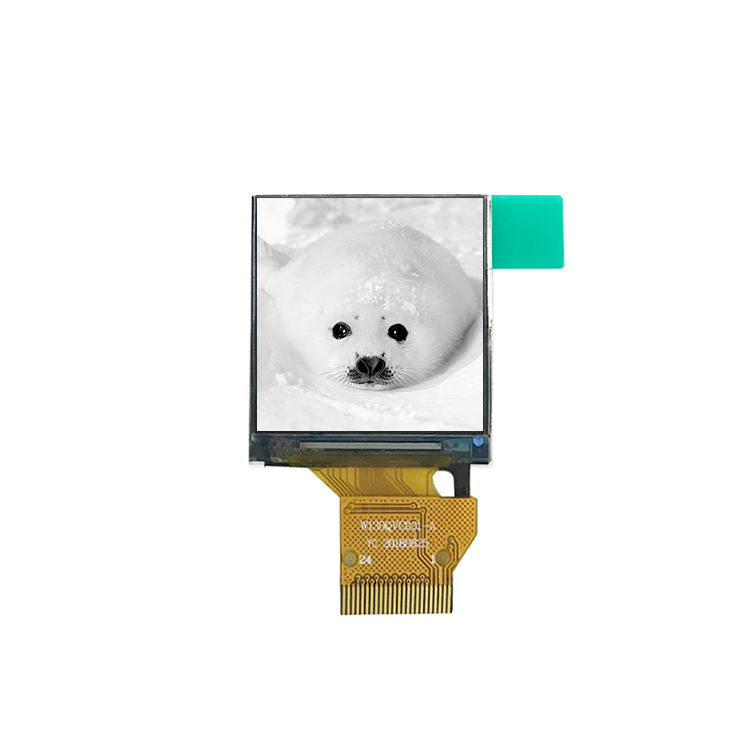
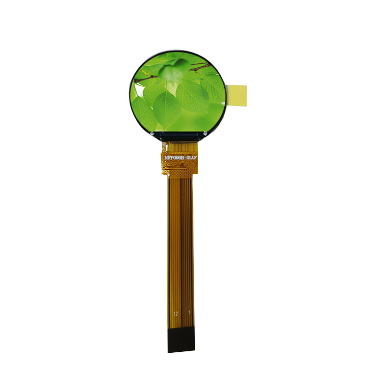
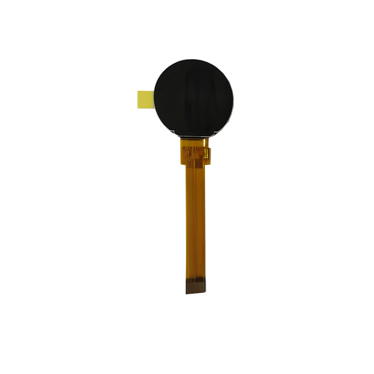
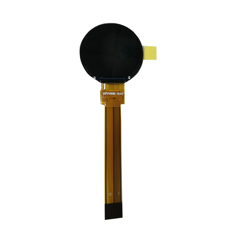
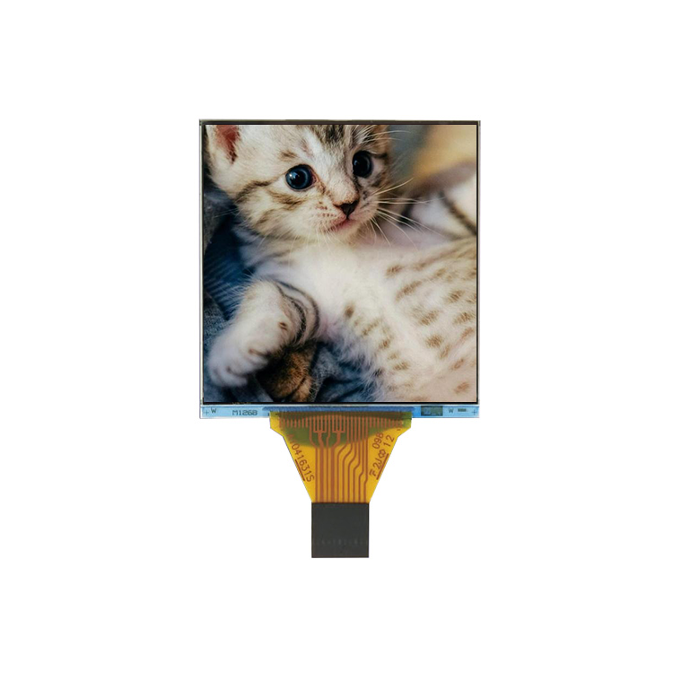
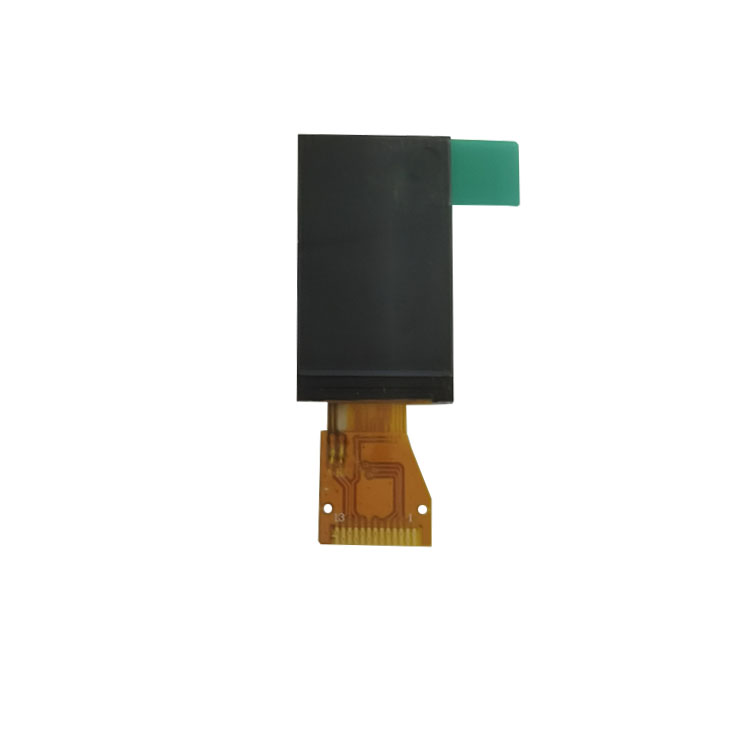
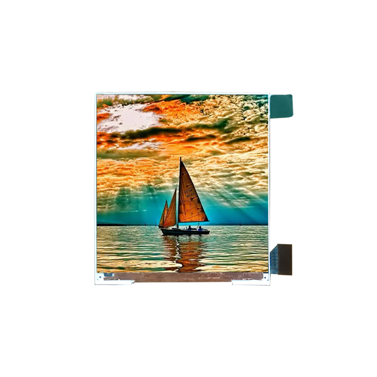
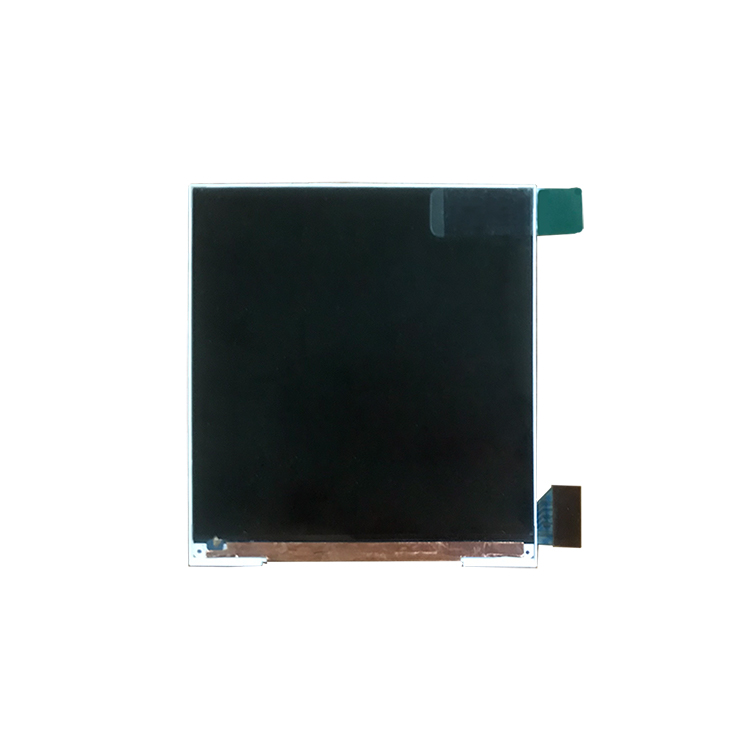
The FPC/Interface/luminance/Touch panel/Cover glass of our most products is customizable.
If you have any requirements, please contact us.
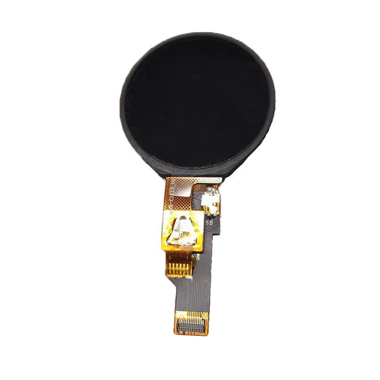
S099KBWPG01-C12 is 0.99 inch IPS All o’clock viewing angle tft lcd display screen with SPI interface. The shape is a circular with resolution 128*115. Outline dimension is 26.71 x 26.22.1mm, thickness is 1.86mm. Active area is 24.36 x 21.89mm. Driver IC is GC9107.Working temperature is -20 to +70℃, storage temperature is -30 to +80℃.
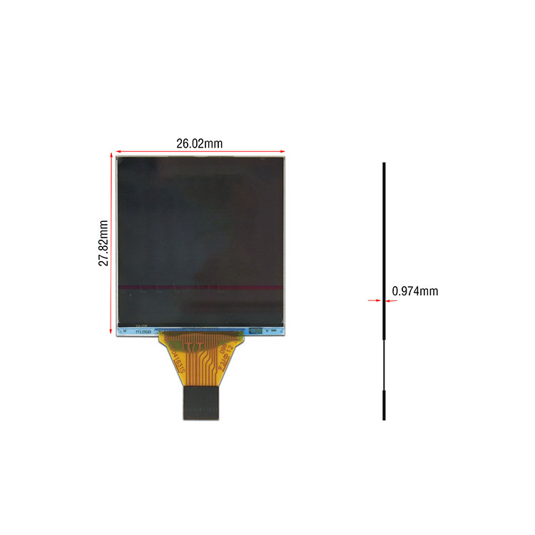
DRAWING
SPECIFICATIONS
| General Specification | |
|---|---|
| Part No. | S099KBWPG01-C12 |
| Outline Dimension(mm) | 26.71(H) x 26.22(V) x1.86(D) |
| Active Area(mm) | 24.36096*21.8868 |
| Number of Pixel(pixels) | 128(H)RGB x 115(V) |
| Touch panel | without |
| Operating temperature(°C) | -20 ~ 70℃ |
| Storage temperature(°C) | -30 ~ +80℃ |
| Driver IC | GC9107 |
| Luminance(cd/m2) | 450 (TYP) |
| Color arrangement | RGB Vertical Stripe |
| Display mode | Normally Black |
| Interface | SPI 4 interface |
| Viewing Direction | ALL o'clock |
| Backlight | 2 White LED |
| Weight(g) | 1.2 |
| Pins Description | ||
|---|---|---|
| PIN NO. | Symbol | Description |
| 1 | GND | Power Ground |
| 2 | LEDK | LED Cathode |
| 3 | LEDA | LED Anode |
| 4 | VDD | Power Supply for Analog |
| 5 | GND | Power Ground |
| 6 | GND | Power Ground |
| 7 | D/C | Display data/command selection pin in 4-line serial interface. |
| 8 | CS | Chip selection pin;Low enable,high disable. |
| 9 | SCL | This pin is used to be serial interface clock |
| 10 | SDA | SPI interface input/output pin.the data is latched on the rising edge of the SCL signal. |
| 11 | RESET | This signal will reset the device and it must be applied to properly initialize the chip.Signal is active low. |
| 12 | GND | Power Ground |


