


The FPC/Interface/luminance/Touch panel/Cover glass of our most products is customizable.
If you have any requirements, please contact us.
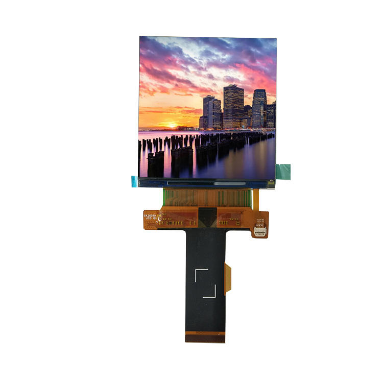
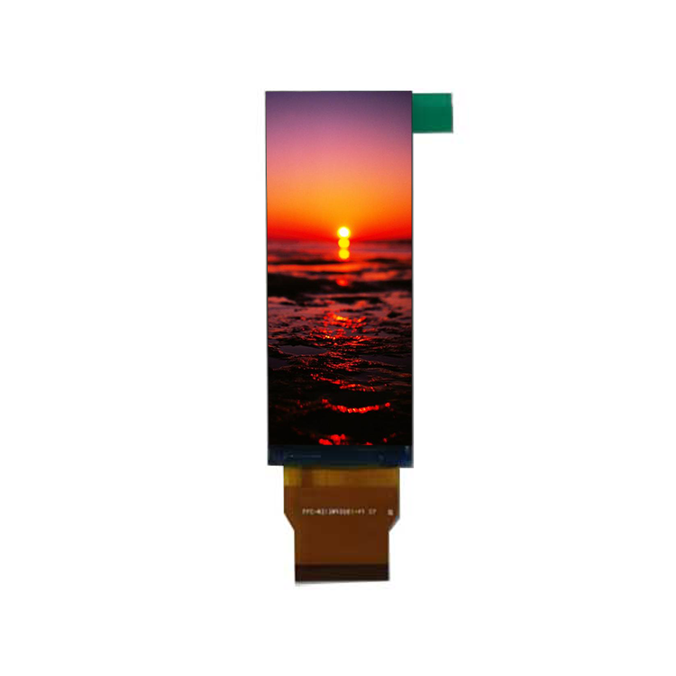
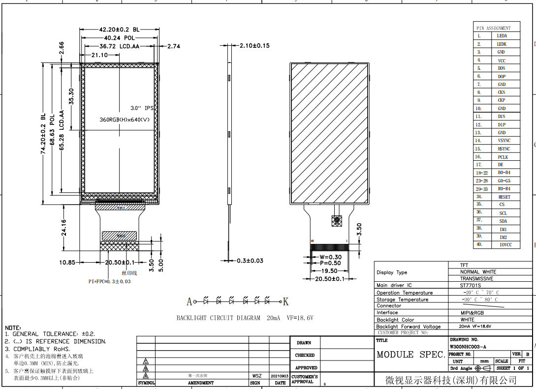
W300NHC003-A is 3 inch tft lcd display module with MIPI&RGB interface and IPS All o’clock viewing angle screen. Customization is available. The shape is a rectangle with resolution 360*640. Outline dimension is 42.20 X 74.20 mm, thickness is 2.1 mm. Active area is 36.72 X 65.28 mm. This lcd display is coming out with 40 pins definition. Working temperature is -20 to +70℃, storage temperature is -30 to +80℃.
DRAWING
SPECIFICATIONS
| General Specification | |
|---|---|
| Part No. | W300NHC003-A |
| LCM Outline Dimension(mm) | 42.20(H) X 74.20(V) X 2.10(T) |
| Active Area(mm) | 36.72(H) X 65.28(V) |
| Number of Pixel(pixels) | 360X(RGB) X 640 |
| Touch panel | without |
| Operating temperature(°C) | -20 ~ 70℃ |
| Storage temperature(°C) | -30 ~ 80℃ |
| Interface | MIPI+RGB |
| Driver IC | ST7701S |
| Display Mode | Normally Black, Transmissive |
| Backlight | White LED |
| Viewing Direction | ALL o'clock |
| Pixel Configuration | RGB Stripe |
| Pins Description | ||
|---|---|---|
| PIN NO. | Symbol | Description |
| 1 | LEDA | Backlight anode. |
| 2 | LEDK | This pin is used to be serial interface clock. |
| 3 | GND | Power ground. |
| 4 | VCC | Analog power supply,2.5V~3.3V. |
| 5 | DON | Negaitive polarity of low voltage differential data signal. |
| 6 | DOP | Positive polarity of low voltage differential data signal. |
| 7 | GND | Power ground. |
| 8 | CLKN | Negaitive polarity of low voltage differentialclock signal. |
| 9 | CLKP | Positive polarity of low voltage differential clock signal. |
| 10 | GND | Power ground. |
| 11 | D1N | Negaitive polarity of low voltage differential data signal. |
| 12 | D1P | Positive polarity of low voltage differential data signal. |
| 13 | GND | Power ground. |
| 14 | VSYNC | Vertical synchronizing input signal for RGB interface operation. |
| 15 | HSYNC | Horizontal synchronizing input signal for RGB interface operation. |
| 16 | PCLK | Dot clock signal for RGB interface operation. |
| 17 | DE | Data enable signal for RGB interface operation. |
| 18-22 | B0-B4 | R.G.B Blue Data bus. |
| 23-28 | G0-G5 | R.G.B Green Data bus. |
| 29-33 | R0-R4 | R.G.B Red Data bus. |
| 34 | RESET | Reset pin. |
| 35 | CS | Chip selection pin.Low-active. |
| 36 | SCL | SPI interface clock signal. |
| 37 | SDA | SPI interface data input/output pin. |
| 38-39 | IM1-IM2 | 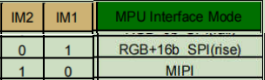 |
| 40 | IOVCC | Interface power supply,1.65v~3.3V. |