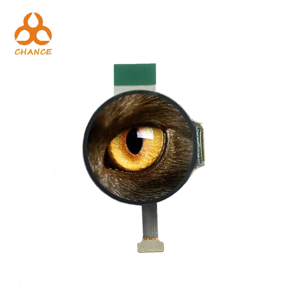
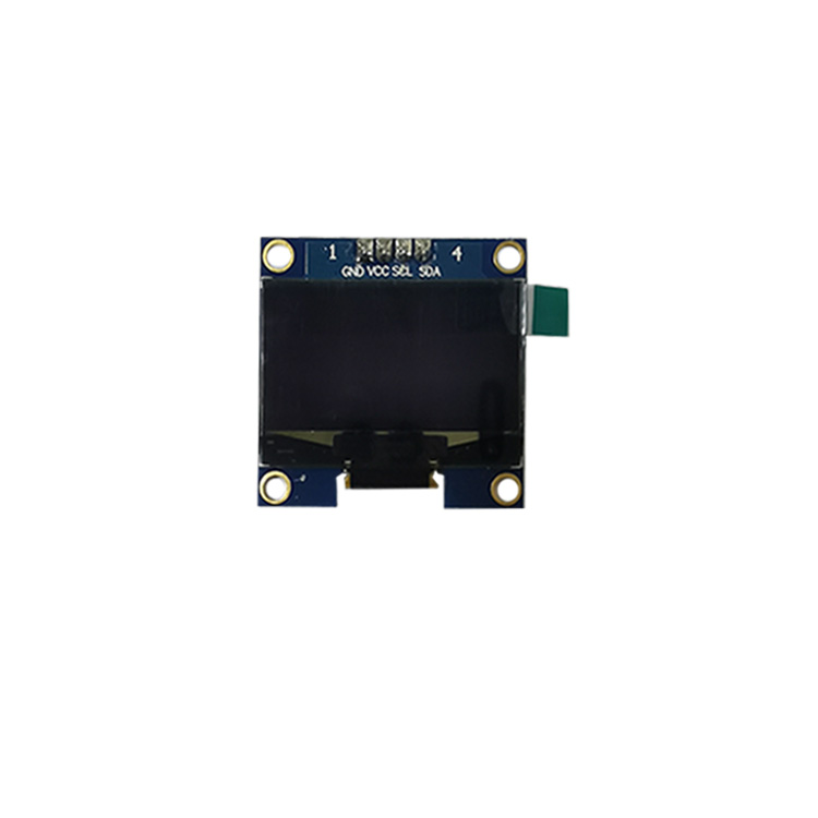
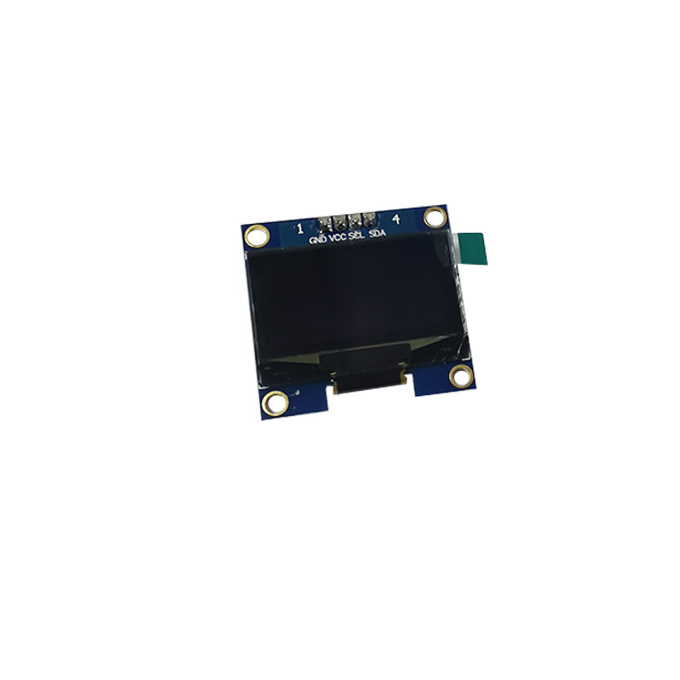
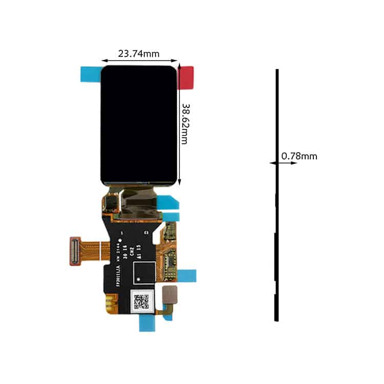
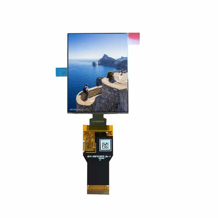
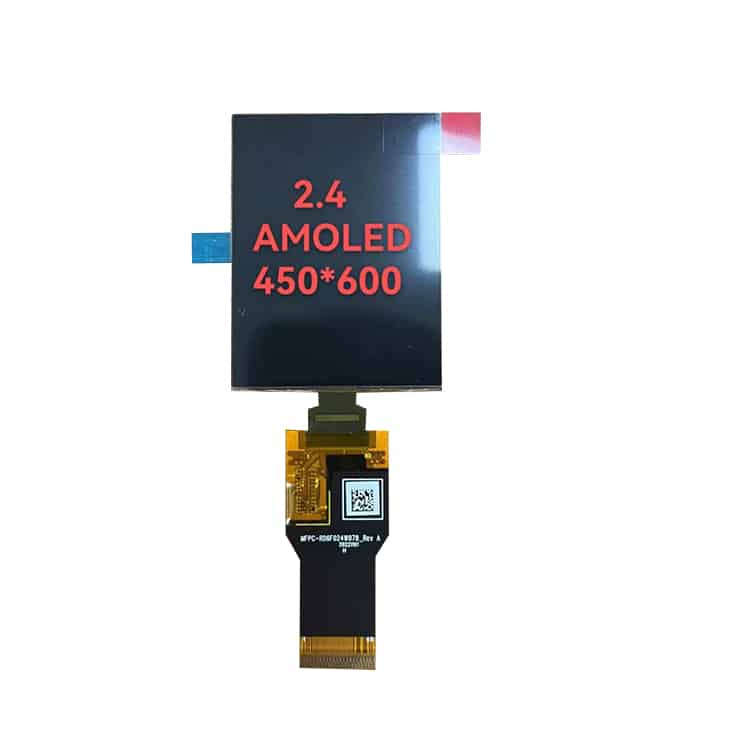
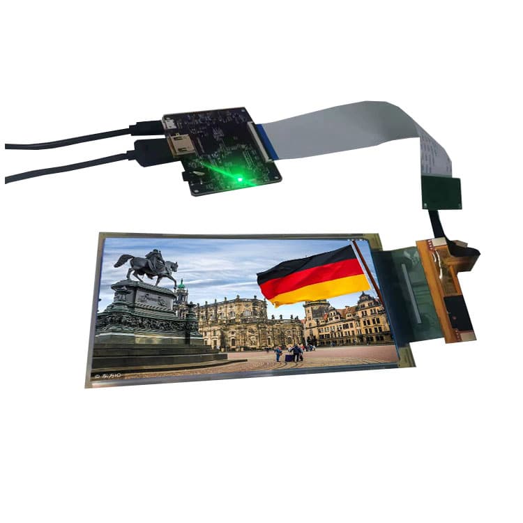
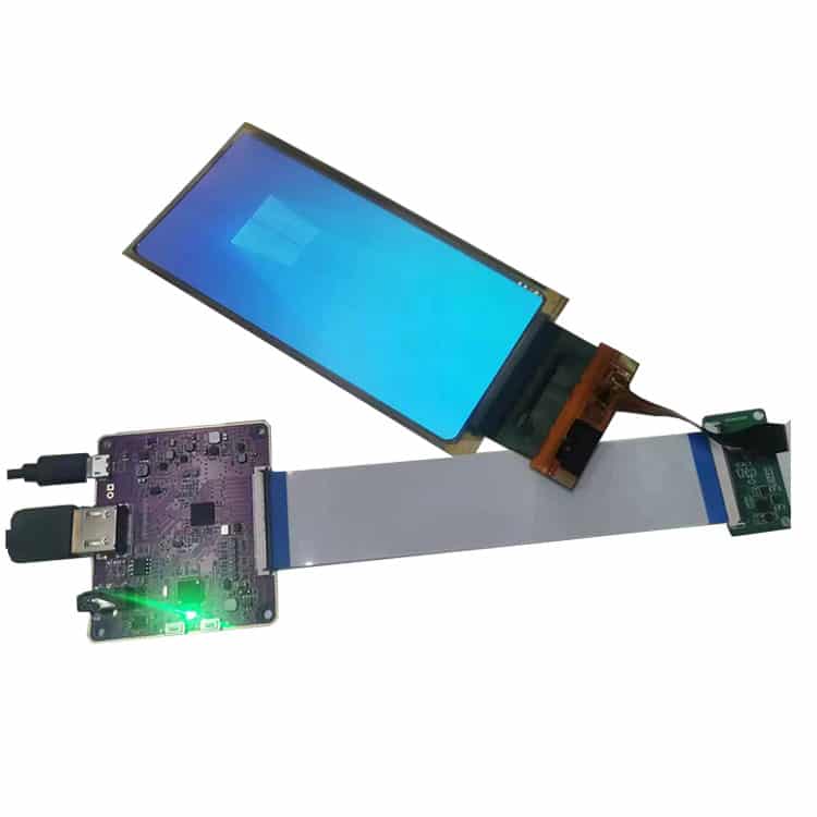
The FPC/Interface/luminance/Touch panel/Cover glass of our most products is customizable.
If you have any requirements, please contact us.
This 7.8-inch flexible AMOLED panel features a high resolution of 1440×1920, vibrant colors, and high brightness, offering exceptional visual quality. Its bendable design makes it perfect for innovative applications like foldable devices, wearable technology, and dynamic displays.
DRAWING

SPECIFICATIONS
| General Specification | |
|---|---|
| Part No. | 7.8 Inch Flexible OLED |
| Place of Origin | Guangdong, China |
| Brand Name | Chance |
| Type | OLED |
| Size | 7.8 Inch |
| Resolution | 1440* 1920 |
| Interface | MIPI |
| Color depth | 16.7 M (3*8bit) |
| Brightness | 300cd/m2 |
| Power consumption | 2.7W @ 300 nits Full White |
| PPI | 308 |
| Operating Temperature | -20~70°C |
| Storage Temperature | -30-70°C |
| Backlight | White LED |
| Module lifetime(Hours) | 50000 |
| PIN No. | Symbol | I/O | Descriptions |
|---|---|---|---|
| 1 | ELVDD FB | p | ELVDD Sense Pin For Power IC FeedBack |
| 2 | NC | - | NC |
| 3 | AVDD | p | Power supply for analog circuit and driver output |
| 4 | NC | - | NC |
| 5 | NC | - | NC |
| 6 | GND | p | Ground |
| 7 | VCI | p | Power supply for analog system & TP |
| 8 | NC | - | NC |
| 9 | VDDIO | p | Power supply for digital system & TP |
| 10 | GND | p | Ground |
| 11 | RSTX | I | Reset for AMOLED SIGNAL |
| 12 | EN | 0 | Power IC enable control pin, If not used, Please leave this pin ope n |
| 13 | SWIRE | 0 | Swire protocol setting pin of power IC, If not used, Please leave this pin open |
| 14 | GND | p | Ground |
| 15 | P1 D3P | I | DSI-D3+differential data signals of Port 1 |
| 16 | P1 D3N | I | DSI-D3-differential data signals of Port 1 |
| 17 | GND | p | Ground |
| 18 | P1 CLKP | I | CLK+ differential clock signals of Port 1 |
| 19 | P1 CLKN | I | CLK- differential clock signals of Port 1 |
| 20 | GND | p | Ground |
| 21 | P1 D0P | I | DSI-DO+differential data signals of Port 1. |
| 22 | P1 D0N | I | DSI-DO-differential data signals of Port 1. |
| 23 | GND | p | Ground |
| 24 | P0 D2P | I | DSI-D2+differential data signals of Port 0. |
| 25 | P0 D2N | I | DSI-D2-differential data signals of Port 0. |
| 26 | GND | P | Ground |
| 27 | P0 D1P | I | DSI-D1+differential data signals of Port 0. |
| 28 | P0 D1N | I | DSI-D1-differential data signals of Port 0. |
| 29 | GND | P | Ground |
| 30 | GND | P | Ground |
| 31 | P0 D0N | I | DSI-DO-differential data of Port 0. |
| 32 | P0 D0P | I | DSI-DO+differential data of Port 0. |
| 33 | GND | P | Ground |
| 34 | P0 CLKN | I | CLK- differential clock signals of Port 0. |
| 35 | P0 CLKP | I | CLK+ differential clock signals of Port 0 |
| 36 | GND | P | Ground |
| 37 | P0 D3N | I | DSI-D3-differential data of Port 0. |
| 38 | P0 D3P | I | DSI-D3+differential data of Port 0. |
| 39 | GND | P | Ground |
| 40 | P1 D1N | I | DSI-D1-differential data of Port 1. |
| 41 | P1 D1P | I | DSI-D1+differential data of Port 1. |
| 42 | GND | P | Ground |
| 43 | P1 D2N | I | DSI-D2-differential data of Port 1. |
| 44 | P1 D2P | I | DSI-D2+differential data of Port 1. |
| 45 | GND | P | Ground |
| 46 | NC | - | NC |
| 47 | TE | 0 | TE for TP SIGNAL |
| 48 | INT18 | 0 | I NT for TP SIGNAL(1,8V Logic Level) |
| 49 | RST18 | I | Reset for TP SIGNAL(1.8V Logic Level) |
| 50 | SDA18 | I/O | SDA for TP SIGNAL(1.8V Logic Level) |
| 51 | SCL18 | I/O | SCL for TP SIGNAL(1.8V Logic Level) |
| 52 | NC | - | NC |
| 53 | GND | p | Ground |
| 54 | NC | - | NC |
| 55 | NC | - | NC |
| 56 | GND | p | Ground |
| 57 | SPI SDI | I/O | SDI for De-Mura FLASH, Please leave this pin open |
| 58 | SPI SDO | 0 | SDO for De-Mura FLASH, Please leave this pin open |
| 59 | SPI CSN | I | CS for De-Mura FLASH, Please leave this pin open |
| 60 | SPI SCLK | I/O | CLOCK for De-Mura FLASH, Please leave this pin open |
| 61 | ELVDD | p | OLED Positive Power |
| 62 | GND | G | Ground |


