


The FPC/Interface/luminance/Touch panel/Cover glass of our most products is customizable.
If you have any requirements, please contact us.
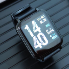
ZB024JMV-N50-6DP0 is 2.4 inch oled display screen with All viewing angle screen. It is SPI/MCU/MIPI interface and resolution is 450*600.Driver IC is RM690B0.Outline dimension is 38.72*51.56 mm, thickness is 0.5mm. Active area is 36.72*48.96 mm. This lcd display is coming out with 45 pins definition. Operating Temperature is -20~80℃, Storage Temperature is -40~80℃.
DRAWING

SPECIFICATIONS
| General Specification | |
|---|---|
| Part No. | ZB024JMV-N50-6DP0 |
| Size | 2.4 inch |
| LCM Outline Dimension(mm) | 38.72*51.56*0.5 |
| Active area | 36.72*48.96 |
| Number of Pixel(pixels) | 450RGB*600 |
| Operating temperature(°C) | -20 ~ 80℃ |
| Storage temperature(°C) | -40~ 80℃ |
| LCD Driver IC | RM690B0 |
| Viewing Direction | All direction |
| Color | 16.7M(24bit) |
| Display mode | Active Matrix |
| Interface | SPI/MCU/MIPI |
| Contrast ratio | 100000:1 |
| Brightness | 800nits |
| Pins Description | |||
|---|---|---|---|
| Pin No. | Symbol | I/O | Function Description |
| 1 | GND | Power | Ground. |
| 2 | GND | Power | Ground. |
| 3 | ELVSS | Power | Negative Power supply for Panel |
| 4 | ELVSS | Power | Negative Power supply for Panel |
| 5 | GND | Power | Ground. |
| 6 | ELVDD | Power | Positive Power supply for Panel |
| 7 | ELVDD | Power | Positive Power supply for Panel |
| 8 | GND | Power | Ground. |
| 9 | VCI | Power | Power supply for display driver IC analog system. |
| 10 | GND | Power | Ground. |
| 11 | VDDIO | Power | Power supply for display driver IC interface and logic system |
| 12 | GND | Power | Ground. |
| 13 | TE1 | O | IC Status active reporting pin. |
| 14 | SWIRE | O | Swire protocol setting pin of Power IC |
| 15 | TE | O | Tearing effect output pin to synchronize MCU to frame writing, activated by S/W command. When this pin is not activated, this pin is output low. |
| 16 | RESX | I | Display driver reset, must be applied to properly initialize the chip. Signal is active low. |
| 17 | GND | Power | Ground. |
| 18 | SDI_RDX | I/O | SDI: Serial input signal in SPI I/F. The data is input on the rising edge of the SCL signal. RDX: Reads strobe signal to write data when RDX is “Low” in 80-series MPU interface. |
| 19 | DCX | I | Display data / command selection in 80-series MPU I/F and 4-wire SPI I/F. |
| 20 | SCL | I | WRX : Writes strobe signal to write data when WRX is “Low” in 80-series MPU I/F. SCL: A synchronous clock signal in SPI I/F. |
| 21 | CSX | I | Chip select input pin (“Low” enable) in 80-series MPU I/F and SPI I/F. |
| 22-29 | D0-D7 | I/O | 8-bit bi-directional data bus for 80-series MPU I/F and 8-bit input data bus for RGB I/F. |
| 30 | GND | Power | Ground. |
| 31 | IM1 | I | Interface type selection. |
| 32 | IM0 | I | Interface type selection. |
| 33 | GND | Power | Ground. |
| 34 | GND | Power | Ground. |
| 35 | D0P | I/O | Differential data signals if MIPI interface. |
| 36 | D0N | I/O | Differential data signals if MIPI interface. |
| 37 | GND | Power | Ground. |
| 38 | GND | Power | Ground. |
| 39 | CLKP | I | Differential clock signals if MIPI interface. |
| 40 | CLKN | I | Differential clock signals if MIPI interface. |
| 41 | GND | Power | Ground. |
| 42 | GND | Power | Ground. |
| 43 | MTP | Power | MTP programming power supply. Must be left open or connected to GND in normal condition. |
| 44 | GND | Power | Ground. |
| 45 | GND | Power | Ground. |
 .
.


