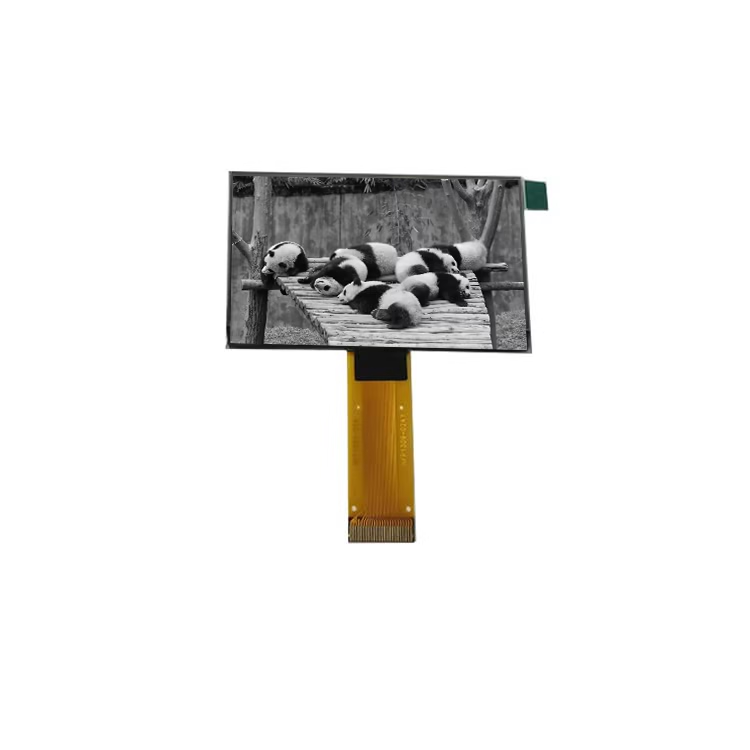
G1392FH101GG-003 is 3.92 inch oled display screen with wide viewing angle screen. It is MIPI interface and resolution is 1080*1240.Driver IC is RM692C9.Outline dimension is 67.248×79.874 mm, thickness is 0.699mm. Active area is 65.448 × 75.144 mm. This oled is coming out with 34 pins definition. Operating Temperature is -20~70℃, Storage Temperature is -30~80℃.
DRAWING


SPECIFICATIONS
| General Specification | |
|---|---|
| Part No. | G1392FH101GG-003 |
| Outline Dimension(mm) | 67.248(W)x79.874(H)x0.699(D) |
| Active Area(mm) | 65.448 (W) × 75.144 (H) |
| Number of Pixel(pixels) | 1080(H) × 1240(V) |
| Operating temperature(°C) | -20 ~ +70℃ |
| Storage temperature(°C) | -30 ~ +80℃ |
| Display color | Full Color (16.7M color) |
| Display mode | Active Matrix |
| Interface | MIPI |
| Viewing Angle | Wide view (85˚/85˚/85˚/85˚) |
| Driver IC | RM692C9 |
| Pins Description | |||
|---|---|---|---|
| PIN | Symbol | I/O | Description |
| 1 | VCI | P | Power supply for display analog circuits |
| 2 | GND | GND | Ground |
| 3 | VDDIO | P | Power supply for interface system except MIPI interface |
| 4 | RSTX | I | Display reset.Active low. |
| 5 | TE | O | Sync Signal for preventing Tearing Effect |
| 6 | ERR_FG | O | Error status of MIPI's HSDT |
| 7 | NC | - | NC |
| 8 | GND | GND | Ground |
| 9 | AVDD | P | Power supply for Analog system |
| 10 | GND | GND | Ground |
| 11 | ELVDD | P | Positive power supply for EL |
| 12 | ELVDD | P | Positive power supply for EL |
| 13 | ELVDD | P | Positive power supply for EL |
| 14 | GND | GND | Ground |
| 15 | ELVSS | P | Negative power supply for EL |
| 16 | ELVSS | P | Negative power supply for EL |
| 17 | ELVSS | P | Negative power supply for EL |
| 18 | GND | GND | Ground |
| 19 | TP_INT | I | Interrupt signal for TP |
| 20 | TP_RESET | I | Reset Pin for TP,Active low |
| 21 | TP_SDA | I/O | SDA pin for TP |
| 22 | TP_SCL | I | SCL pin for TP |
| 23 | GND | GND | Ground |
| 24 | VPP | P | Power supply for MTP Programming or Erase. lf it is not used, please let it open |
| 25 | TP_1P8 | P | Digital Power for TP |
| 26 | TSP_AVDD | P | Analog Power for TP |
| 27 | GND | GND | Ground |
| 28 | D3N | I | MIPI data lane |
| 29 | D3P | I | MIPI data lane |
| 30 | GND | O | Control signal for power IC |
| 31 | D0N | I | MIPI data lane |
| 32 | D0P | I | MIPI data lane |
| 33 | GND | GND | Ground |
| 34 | CLKN | I | MIPI clock lane |