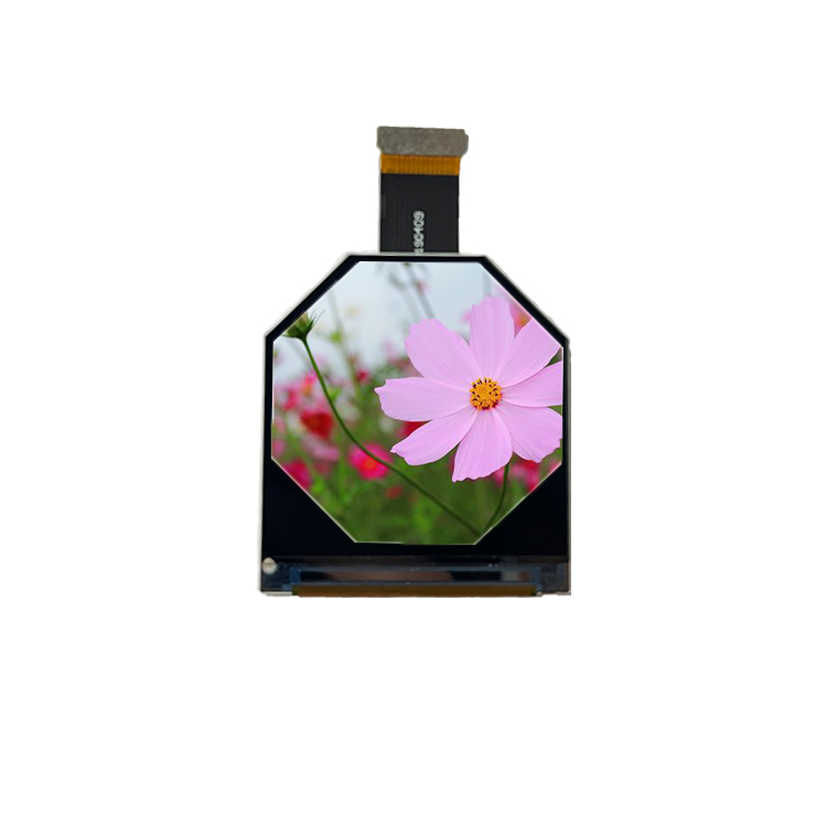
The FPC/Interface/luminance/Touch panel/Cover glass of our most products is customizable.
If you have any requirements, please contact us.
BF051FBM-AK1-7D01 is 5.1 inch oled display screen with flexible screen. It is MIPI interface and resolution is 720*1520.Outline dimension is 57.604×120.584 mm, thickness is 0.7 mm. Active area is 55.404×116.964mm. This oled display is coming out with 44 pins definition. Operating Temperature is -20~70℃, Storage Temperature is -40~80℃.
DRAWING


SPECIFICATIONS
| General Specification | |
|---|---|
| Part No. | BF051FBM-AK1-7D01 |
| Outline Dimension(mm) | 57.604(W) ×120.584(H)×0.13(T) |
| Active Area(mm) | 55.404(W) ×116.964(H) |
| Number of Pixel(pixels) | 720(W) ×RGB ×1520(H) |
| Operating temperature(°C) | -20 ~ +70℃ |
| Storage temperature(°C) | -40 ~ +80℃ |
| Pixel Arrangement | RGB |
| Display mode | Active Matrix |
| Interface | MIPI-DSI 4 lanes |
| Driver IC | RM692F9 |
| Brightness | 350nits |
| Polarizer | CPOL(with PSA)+Flexible Touch Sensor |
| Pins Description | ||
|---|---|---|
| PIN | Symbol | Description |
| 1 | GND | GND PIN |
| 3 | D3N | MIPI Data Lane 3- |
| 5 | D3P | MIPI Data Lane 3+ |
| 7 | GND | GND PIN |
| 9 | DON | MIPI Data Lane 0- |
| 11 | DOP | MIPI Data Lane 0+ |
| 13 | GND | GND PIN |
| 15 | CKN | MIPI CLK Lane- |
| 17 | CKP | MIPICLK Lane + |
| 19 | GND | GND PIN |
| 21 | D1N | MIPI Data Lane 1- |
| 23 | D1P | MIPI Data Lane 1+ |
| 25 | GND | GND PIN |
| 27 | D2N | MIPI Data Lane 2+ |
| 29 | D2P | MIPI Data Lane 2- |
| 31 | GND | GND PIN |
| 33 | ID (GND) | ID PIN |
| 35 | NC | NC |
| 37 | ELVSS | EL Low power |
| 39 | ELVSS | EL Low power |
| 2 | VPP(MTP_PWR) | MTP Power |
| 4 | ELON2(SWIRE) | Swire PIN(communication to DCDC) |
| 6 | VDDP EN(OLEN EN) | EN PIN(Enable signal communication to DCDC |
| 8 | TE | TE Flag PIN(communication to AP) |
| 10 | ERR FG | ERR Flag Pin(communication to AP) |
| 12 | RESX(RETN) | Reset Signal |
| 14 | VDDI | 1.8V VDDIO Power |
| 16 | NC | NC |
| 18 | VLIN1_7.6V(AVDD) | AVDD POWER |
| 20 | NC | NC |
| 22 | VCI 3.0V | VCI POWER |
| 24 | TSP AVDD 3.3V | TSP Analog power |
| 26 | NC | NC |
| 28 | TSP SDA | TSP Data Lane |
| 30 | TSP_SCL | TSP CLK Lane |
| 32 | TSP_INT | TSP initial signal PIN |
| 34 | TSP_RESET | TSP Reset PIN |
| 36 | NC | NC |
| 38 | ELVDD | EL High Power |
| 40 | ELVDD | EL High Power |
| 41 | GND | GND |
| 42 | GND | GND |
| 43 | GND | GND |
| 44 | GND | GND |