The FPC/Interface/luminance/Touch panel/Cover glass of our most products is customizable.
If you have any requirements, please contact us.
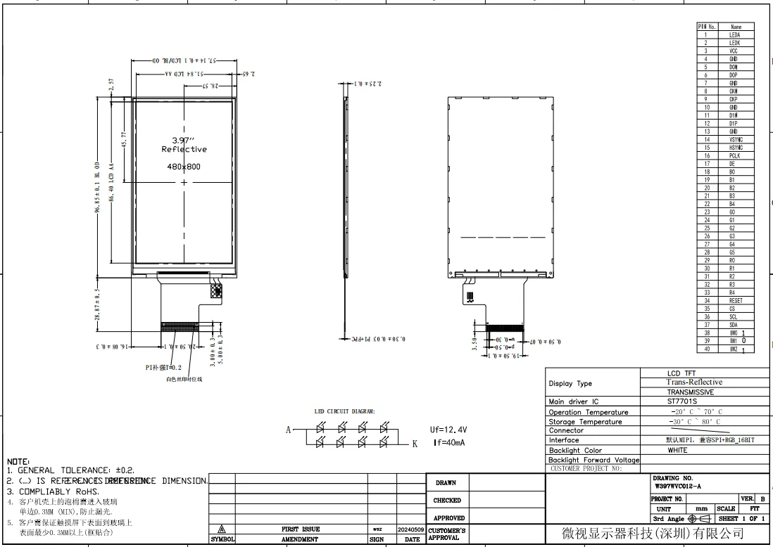
W397WVC012-A is 3.97 inch Transflective lcd display module with MIPI/SPI+RGB interface and ALL o’clock viewing angle screen. Customization is available. The shape is a rectangle with resolution 480*800. Outline dimension is 57.14*96.85 mm, thickness is 2.25 mm. Active area is 51.84(H)*86.40(V) mm. This lcd display is coming out with 40 pins definition. Working temperature is -20 to +70℃, storage temperature is -30 to +80℃.
DRAWING
SPECIFICATIONS
| Item | Specification | Unit |
|---|---|---|
| Part No. | W280TRQVC001-A | - |
| Display Mode | Normally Black, Trans-Reflective | - |
| Display Technology | α-Si TFT active matrix | - |
| Outline Dimension | 57.14(H) X 96.85(V) X 2.25(T) | mm |
| Active Area | 51.84 (H) X 86.40 (V) | mm |
| Resolution | 480X(RGB)X800 | dots |
| Pixel Pitch | 0.108(H) × 0.108(V) | mm |
| Pixel Configuration | RGB Stripe | - |
| Backlight | White LED | - |
| LCD Driver IC | ST7701 | - |
| Viewing Direction | FREE o’clock | - |
| Module lifetime(Hours) | 50000 | H |
| Interface NO. | Symbol | Description |
|---|---|---|
| Pin No | Symbol | Functional |
| 1 | LEDA | Power supply for backlight anode input terminal |
| 2 | LEDK | Power supply for backlight cathode input terminal. |
| 3 | VCC | Anulog power supply |
| 4 | GND | Power Ground |
| 5 | D0N | Negative polarity of low voltage differential data signal |
| 6 | D0P | Positive polanty of low voltage differential data signal |
| 7 | GND | Power Ground |
| 8 | CLKN | Negative polarity of low voltage differential clock signal |
| 9 | CLKP | Positive polarity of low voltage differential clock signal |
| 10 | GND | Power Ground |
| 11 | DIN | Negative polarity of low voltage differential data signal |
| 12 | DIP | Positive polarity of low voltage differential data signal |
| 13 | GND | Power Ground |
| 14 | VSYNC | Vertical synchronizing input signal for RGB interface operation. |
| 15 | HSYNC | Horizontal synchronizing input signal for RGB interface operation. |
| 16 | PCLK | Dot clock signal for RGB interface operation. |
| 17 | DE | Data enable signal for RGB interface operation. |
| 18-22 | B0~B4 | R.G.B Data bus. |
| 23-28 | G0~B5 | R.G.B Data bus. |
| 29-33 | R0~R4 | R.G.B Data bus. |
| 34 | RESET | Reset signal |
| 35 | CS | Chip selection pin.Low-active, |
| 36 | SCL | Clock signal. |
| 37 | SDA | SPI interface input pin. |
| 38 | IM0 | The interface mode select. |
| 39 | IM1 | The interface mode select. |
| 40 | IM2 | The interface mode select. |