


The FPC/Interface/luminance/Touch panel/Cover glass of our most products is customizable.
If you have any requirements, please contact us.
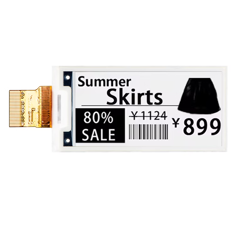
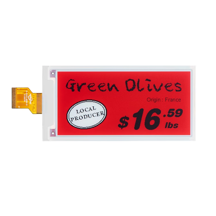
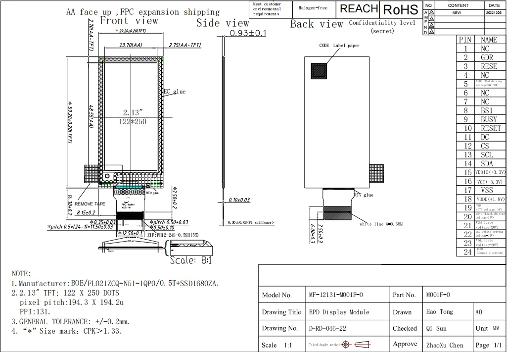
Ink Cubic-M001F-O is an Active Matrix Electrophoretic Display (AMEPD), with interface and a reference system design. The2.13active area contains 122×250pixels, and has 1-bit B/W full display capabilities. An integrated circuit contains gate buffer, source buffer, interface, timing control logic, oscillator, DC-DC, SRAM, LUT, VCOM and border are supplied with each panel
DRAWING
SPECIFICATIONS
| General Specification | |
|---|---|
| Part No. | MF-12131-M001F-O |
| Place of Origin | Guangdong, China |
| Brand Name | Chance |
| Product Name | E Ink Display |
| Outline Dimension | 29.20(H)x59.20(V) xO.93(D) |
| Active Area | 23.7O(H)X48.55(V) |
| Pixel Pitch | 0.194x0.194 |
| Resoluti on | 122*250 |
| Interface | 3-wire SPI/4-wire SPI |
| LCD Driver IC | SSD1680 |
| Display Color | Black White (Optional) |
| Operating Temperature | 0~40°C |
| Storage Temperature | 25~60°C |
| Pin # | Single | Description | Remark |
|---|---|---|---|
| 1 | NC | No connection and do not connect with other NC pins | Keep Open |
| 2 | GDR | N-Channel MOSFET Gate Drive Control | |
| 3 | RESE | Current Sense Input tor the Control Loop | |
| 4 | NC | No connection and do not connect with other NC pins | Keep Open |
| 5 | VSH2 | Positive Source driving voltage | |
| 6 | NC | No connection and do not connect with other NC pins | Keep Open |
| 7 | NC | No connection and do not connect with other NC pins | Keep Open |
| 8 | BS1 | Bus selection pin | Note 6-5 |
| 9 | BUSY | Busy state output p in | Note 6-4 |
| 10 | RES# | Resit signal input | Note 6-3 |
| 11 | D/C# | Data /Command control pin | Note 6-2 |
| 12 | cs# | The chip select input connecting to the MCU. | Note 6-1 |
| 13 | SCL | Serial clock pin tor interface. | |
| 14 | SDA | Serial data pin for interiace. | |
| 15 | VDDIO | Power input pin tor the Interlace. | |
| 16 | VCI | Power Supply pin for the chip | |
| 17 | VSS | Ground (Digital) | |
| 18 | VDD | Core logic power pin | |
| 19 | VPP | Power Supply lor OTP Programmjng | |
| 20 | VSH1 | Positive Source driving voltage | |
| 21 | VGH | Power Supply pin tor Positive Gate driving voltage and VSH | |
| 22 | VSL | Negative Source driving voltage | |
| 23 | VGL | Power Supply pin tor Negative Gate driving voltage, VCOM and VSL | |
| 24 | VCOM | VCOM driving vohage |