


The FPC/Interface/luminance/Touch panel/Cover glass of our most products is customizable.
If you have any requirements, please contact us.
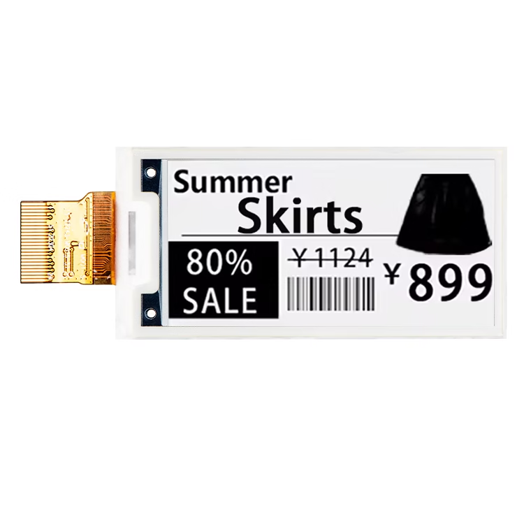
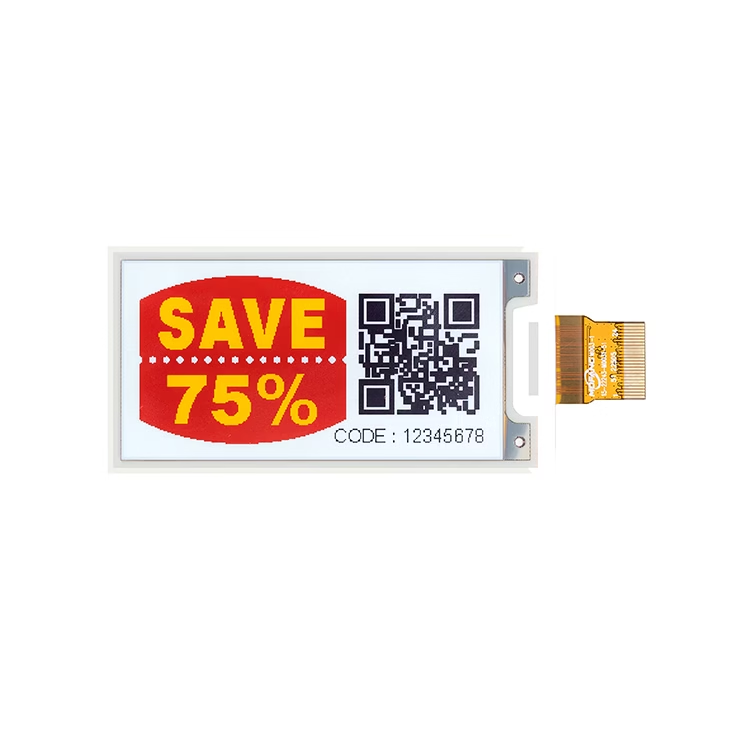
Ink Cubic-M014F is an Active Matrix Electrophoretic Display (AMEPD), with interface and a reference system design. The2.7”active area contains 176×264 pixels, and has 1-bit B/W/R full display capabilities. An integrated circuit contains gate buffer, source buffer, interface, timing control logic, oscillator, DC-DC, SRAM, LUT, VCOM and border are supplied with each panel.
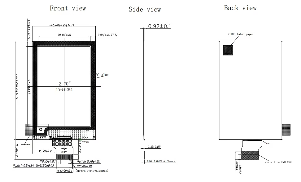
DRAWING
SPECIFICATIONS
| Parameter | Specifications | Unit |
|---|---|---|
| Screen Size | 2.7 | Inch |
| Disphy Resolution | 176(H)x264(V) | Pixel |
| Active Area | 3&!92(H)x57.288(V) | mm |
| Pixel Pitch | 0.217x0.217 | mm |
| Pixel ConiiguratK)n | Rectangle | |
| Outline Dimension | 45.80(H)x70.42(V)x0.92(D) | mm |
| Weight | 5.92±0.5 | g |
| Pin# | Single | Description | Remark |
|---|---|---|---|
| 1 | NC | No connection and do not connect with other NC pins | Keep Open |
| 2 | GDR | N-Channel MOSFET Gate Drive Control | |
| 3 | RESE | Current Sense Input for the Control Loop | |
| 4 | NC | No connection and do not connect with other NC pins | Keep Open |
| 5 | VSH2 | Positive Source driving voltage | |
| 6 | NC | No connection and do not connect with other NC pins | Keep Open |
| 7 | NC | No connection and do not connect with other NC pins | Keep Open |
| 8 | BS1 | Bus selection, pin | Note 6-5 |
| 9 | BUSY | Busy state output pin | Note 6-4 |
| 10 | RES# | Rcsei signal input. | Note 6-3 |
| 11 | D/C# | Data /Command comrol pin | Note 6-2 |
| 12 | CS# | The chip select input connecting to the MCU. | Note 6-1 |
| 13 | SCL | Serial clock pin tor interlace. | |
| 14 | SDA | Serial data pin for interlace. | |
| 15 | VDDIO | Power input pin for the Interface. | |
| 16 | VC1 | Power Supply pin for the chip | |
| 17 | vss | Ground (Digital) | |
| 18 | VDD | Core logic power pin | |
| 19 | VPP | Power Supply lor OTP Pr卑rammi哼 | |
| 20 | VSH1 | Positive Source driving voltage | |
| 21 | VGH | Power Supply pin lor Positive Gate driving voltage and VSH | |
| 22 | VSL | Negative Source driving voltage | |
| 23 | VGL | Power Supply pin for Negative Gate drivi陛 voltage, VCOM and VSL | |
| 24 | VCOM | VCOM driving voltage |