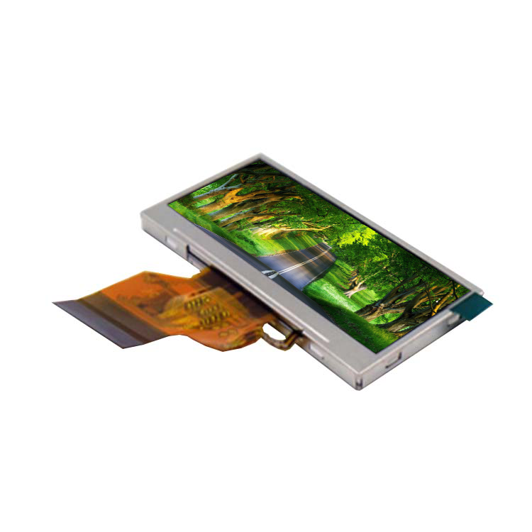
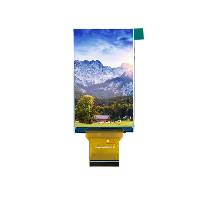
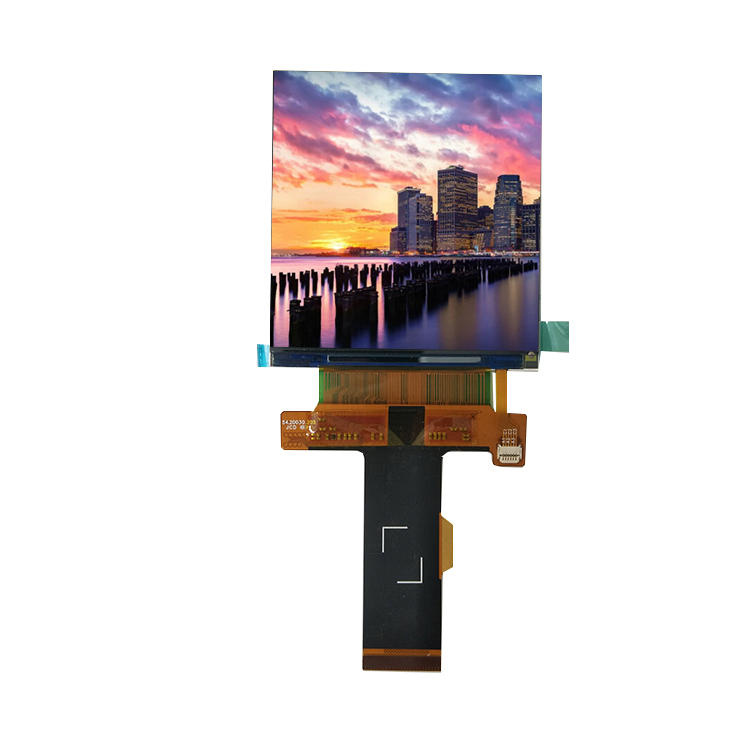
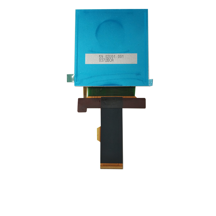
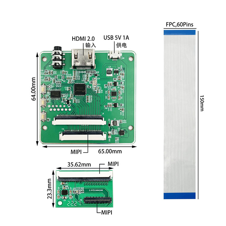
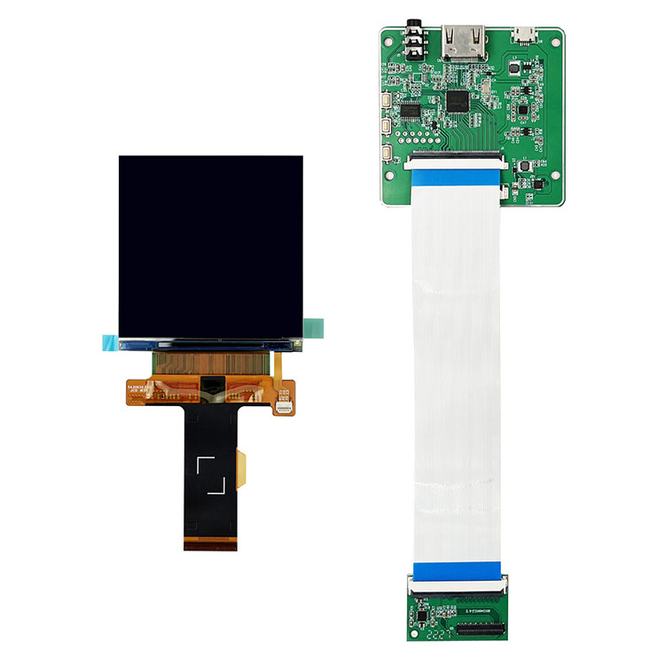
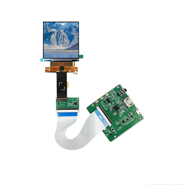
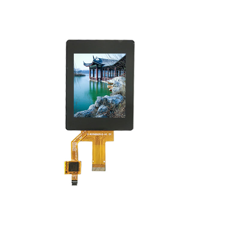
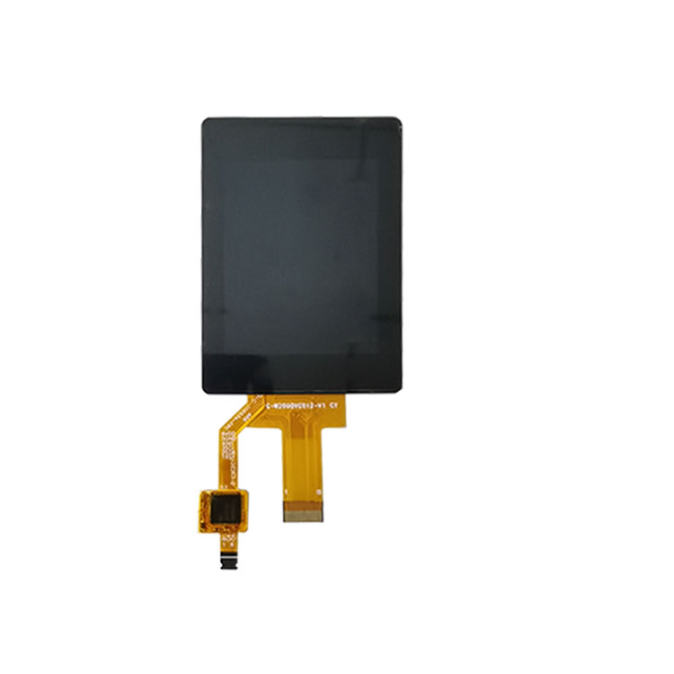
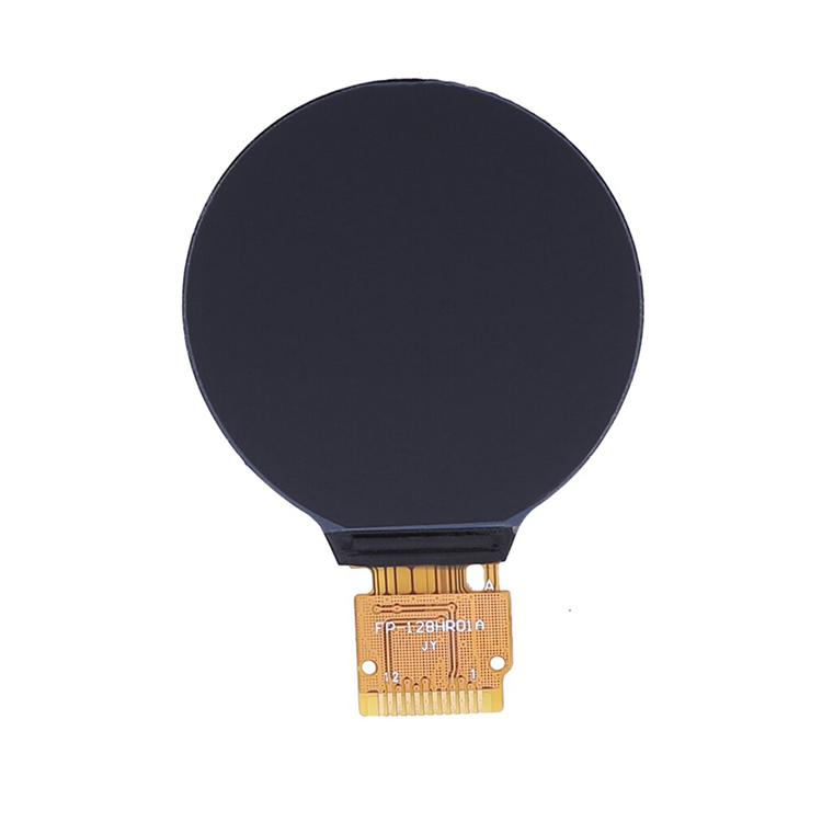
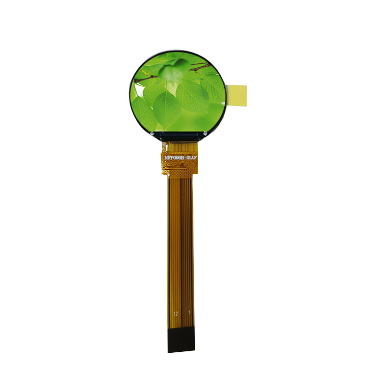
The FPC/Interface/luminance/Touch panel/Cover glass of our most products is customizable.
If you have any requirements, please contact us.
LS029B3SX06 is 2.89 inch tft lcd display module with MIPI interface and IPS All o’clock viewing angle screen. Customization is available. The shape is a square with high resolution 2160*2160. Outline dimension is 54.24 x 59.32mm, thickness is 1.365mm. Active area is 51.84 x 51.84 mm. This lcd display is coming out with 51 pins definition. Working temperature is -10 to +60℃, storage temperature is -20 to +70℃.
DRAWING

SPECIFICATIONS
| General Specification | |
|---|---|
| Part No. | LS029B3SX06 |
| LCM Outline Dimension(mm) | 54.24(W) x 59.32(H) x 1.365(D) |
| Active Area(mm) | 51.84(H) x 51.84(V) |
| Number of Pixel(pixels) | 2160(H) x 2160(V) |
| Touch panel | without |
| Operating temperature(°C) | -10 ~ +60℃ |
| Storage temperature(°C) | -20 ~ +70℃ |
| Driver IC | R63455 |
| Brightness | 100nits |
| Number of colors | 16,777,216 |
| Pixel configuration | R,G,B Vertical Stripes |
| Display mode | Normally Black |
| Interface | MIPI |
| Viewing Direction | All o'clock |
| Pins Description | |||
|---|---|---|---|
| PIN NO. | Symbol | Description | I/O or connect to |
| 1 | VSN | Power supply to the analog circuit (-5.8V) | I |
| 2 | VSN | Power supply to the analog drcuit(-5.8V) | I |
| 3 | VDDIO | Power supply to the logic drcuit (1.8V) | I |
| 4 | VDDIO | Power supply to the logic drcuit (1.8V) | I |
| 5 | VSP | Power supply to the analog drcuit (5.8V) | I |
| 6 | VSP | Power supply to the analog circuit (5.8V) | I |
| 7 | GND | GND=0V | I |
| 8 | BOLIGHT | Control signal for LED backlight (refer to next page) | O |
| 9 | TE-2 | Tearing effect output pin2 | O |
| 10 | TE-1 | Tearing effect output pin1 | O |
| 11 | PNSLV | Selects the master port (*H"=port B,"L*=port A) | I |
| 12 | PN2PTX | Selects the number of D5I-2 ports ("H*=1 port,*L"=2 port) | I |
| 13 | RESET | Reset pin (Low active) | I |
| 14 | GND | GND=0V | I |
| 15 | Data 2P_B | Mipi data2 positive signal of MIPI Port B | I |
| 16 | Data 2NLB | Mipi data2 negative signal of MIPI Port B | I |
| 17 | GND | GND=0V | I |
| 18 | Data 1P_B | Mipi data1 positive signal of MIPI Port B | I |
| 19 | Data 1N_B | Mpi data1 negative signal of MIPI Port B | I |
| 20 | GND | GND=0V | I |
| 21 | CLK P_B | Mipi clock positive signal of MIPI Port B | I |
| 22 | CK N_B | Mipi clock negative signal of MIPI Port B | I |
| 23 | GND | GND=0V | I |
| 24 | Data OP_B | Mipi data0 positive signal of MIPI Port B | I/O |
| 25 | Data ON_B | Mipi data0 negative signal of MIPI Port B | I/O |
| 26 | GND | GND=0V | I |
| 27 | Data 3P_B | Mipi data3 positive signal of MIPI Port B | I |
| 28 | Data 3NLB | Mipi data3 negative signal of MIPI Port B | I |
| 29 | GND | GND=0V | I |
| 30 | Data 3NLA | Mipi data3 negative signal of MIPI Port A | I |
| 31 | Data 3P_A | Mipi data3 positive signal of MIPI PortA | I |
| 32 | GND | GND=0V | I |
| 33 | Data ONLA | Mipi data0 negative signal of MIPI Port A | I/O |
| 34 | Data OP_A | Mipi data0 positive signal of MIPI Port A | I/O |
| 35 | GND | GND=0V | I |
| 36 | CLK N_A | Mipi cock negative signal of MIPI Port A | I |
| 37 | CLK P_A | Mipi dlock positive signal of MIPI Port A | I |
| 38 | GND | GND=0V | I |
| 39 | Data 1NLA | Mipi datal negative signal of MIPI Port A | I |
| 40 | Data 1P_A | Mipi data1 positive signal of MIPI Port A | I |
| 41 | GND | GND=0V | I |
| 42 | Data 2NA | Mipi data2 negative signal of MIPI Port A | I |
| 43 | Data 2P_A | Mipi data2 positive signal of MIPI Port A | I |
| 44 | GND | GND=0V | I |
| 45 | GND | GND=0V | I |
| 46 | LED-C3 | LED cathode 3 | I |
| 47 | LED-A3 | LED-anode 3 | I |
| 48 | LED-C | LED cathode 2 | I |
| 49 | LED-A2 | LED-anode 2 | I |
| 50 | LED-CI | LED cathode 1 | I |
| 51 | LED-A1 | LED-anode 1 | I |


