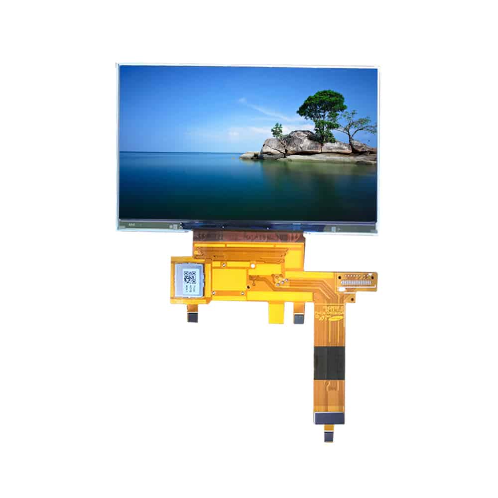
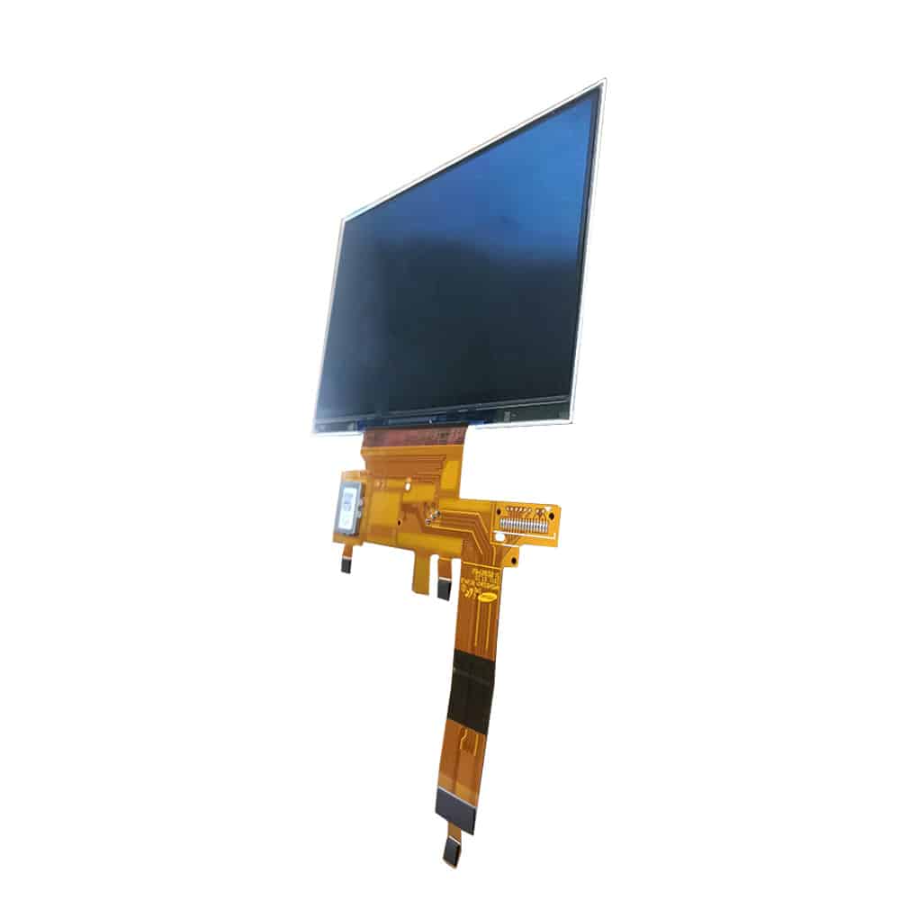
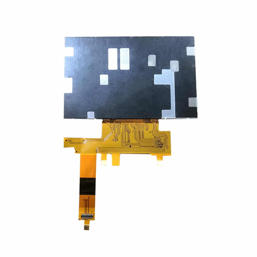
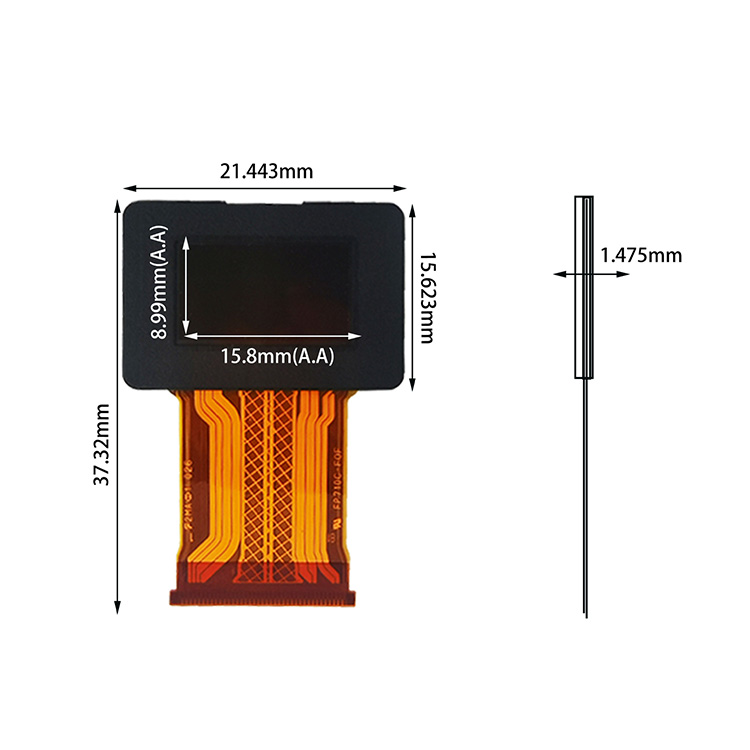
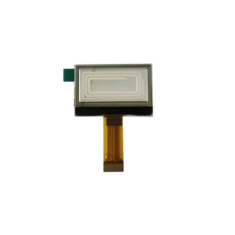
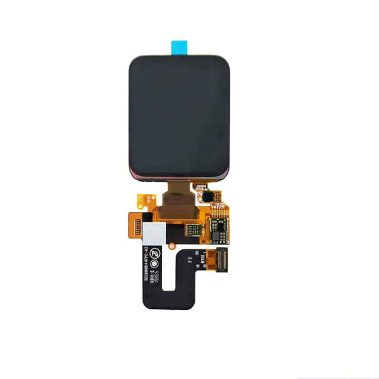
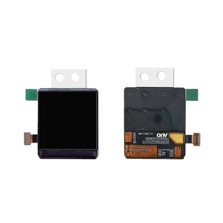
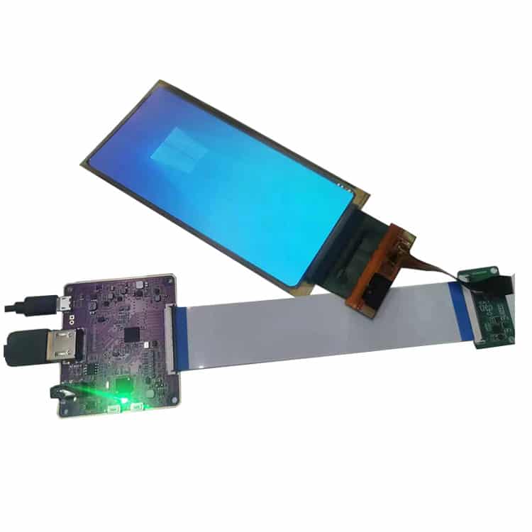
The FPC/Interface/luminance/Touch panel/Cover glass of our most products is customizable.
If you have any requirements, please contact us.
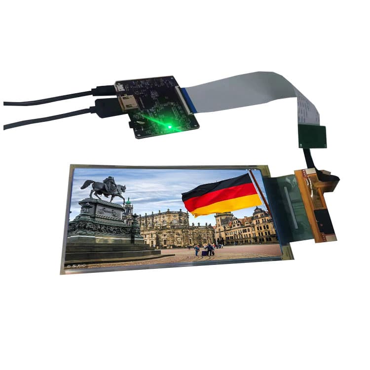
AMS495QA04 is 4.95 inch oled display screen with wide viewing angle screen. It is MIPI and SPI interface. Resolution is 960*544.Outline dimension is 116.54 × 73.92 mm, thickness is 1.66 mm. Active area is 109.44 × 62.02 mm. This oled display is coming out with 40 pins definition. Operating Temperature is -20~70℃, Storage Temperature is -30~85℃.
DRAWING

SPECIFICATIONS
| General Specification | |
|---|---|
| Part No. | AMS495QA04 |
| Outline Dimension(mm) | 116.54(W) X 73.92(H) X 1.66(T) |
| Active Area(mm) | 109.44(W) X 62.02(H) |
| Number of Pixel(pixels) | 960(W) X RGB X 544(H) |
| Operating temperature(°C) | -20 ~ +70℃ |
| Storage temperature(°C) | -30 ~ +85℃ |
| Display color | 16M Color (RGB) |
| Display mode | Active Matrix |
| Interface | SPI(3line), MIPI-DSI(2lane) |
| Driver IC | D53E6EA8966 by Magnachip |
| Brightness | 139cd/m2 |
| Contrast ratio | 6500 |
| Pins Description | |||
|---|---|---|---|
| PIN | Symbol | I/O | Function |
| 1 | VCI | I | Power pin for analog |
| 2 | GND | I | Low voltage ground pin |
| 3 | VCI | I | Power pin for analog |
| 4 | AVDD | I | for TP |
| 5 | VDD | I | Power pin for logic I/O |
| 6 | AVDD | I | for TP |
| 7 | VDD | I | Power pin for logic I/O |
| 8 | GND | I | Low voltage ground pin |
| 9 | GND | I | Low voltage ground pin |
| 10 | ELVDD | I | Power pin for module analog |
| 11 | ELON | O | Module DCDC( ELVDD/ELVSS) on/off control signal( VCI level) |
| 12 | ELVDD | I | Power pin for module analog |
| 13 | RESX | I | Reset pin Initializing when RESX="L" |
| 14 | ELVSS | I | Power pin for module analog |
| 15 | SEL_REG | I | Command& parameter transfer selection “H” transfer by DBI type C(SPI) “L” transfer by DSI type |
| 16 | ELVSS | I | Power pin for module analog |
| 17 | GND | I | Low voltage ground pin |
| 18 | GND | I | Low voltage ground pin |
| 19 | MDN0 | I | DSI interface Data Line 0- |
| 20 | CSX | I | Chip selection pin Data/Command in/out is possible when CSX="L" |
| 21 | MDP0 | I | DSI interface Data Line 0+ |
| 22 | DOUT | I | Serial data input pin |
| 23 | GND | I | Low voltage ground pin |
| 24 | DIN | O | Serial data output pin |
| 25 | MCN | I | DSI interface Strobe clock- |
| 26 | SCL | I | Serial data transfer clock input pin |
| 27 | MCP | I | DSI interface Strobe clock+ |
| 28 | OTPV | - | for SMD internal use only. Open when is not used |
| 29 | GND | I | Low voltage ground pin |
| 30 | GND | I | Low voltage ground pin |
| 31 | MDN1 | I | DSI interface Data Line 1- |
| 32 | TP_SPI_CS | I | for TP |
| 33 | MDP1 | I | DSI interface Data Line 1+ |
| 34 | TP_SPI_MOSI | I | for TP |
| 35 | GND | I | Low voltage ground pin |
| 36 | TP_SPI_MISO | O | for TP |
| 37 | TP_RESET | I | for TP |
| 38 | TP_SPI_CLK | I | for TP |
| 39 | TP_INT | I | for TP |
| 40 | GND | I | Low voltage ground pin |


