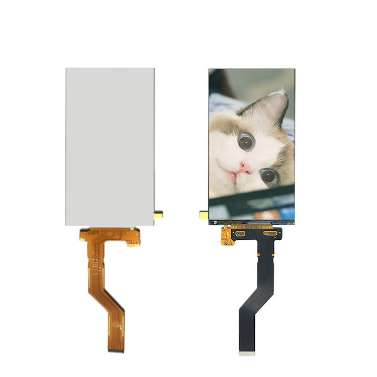
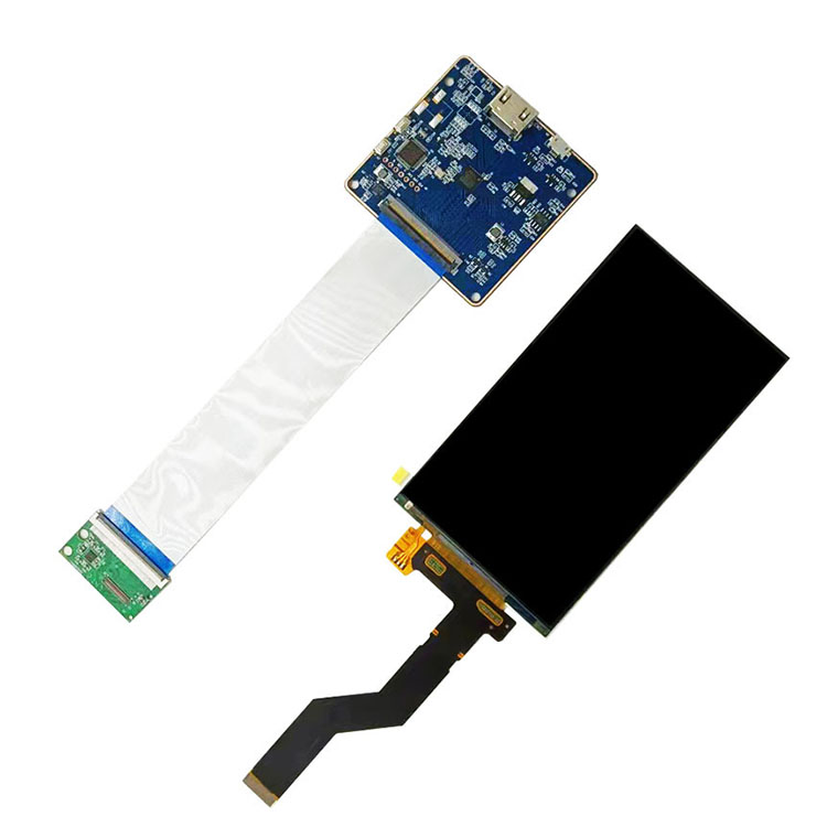
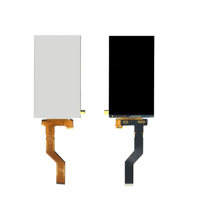
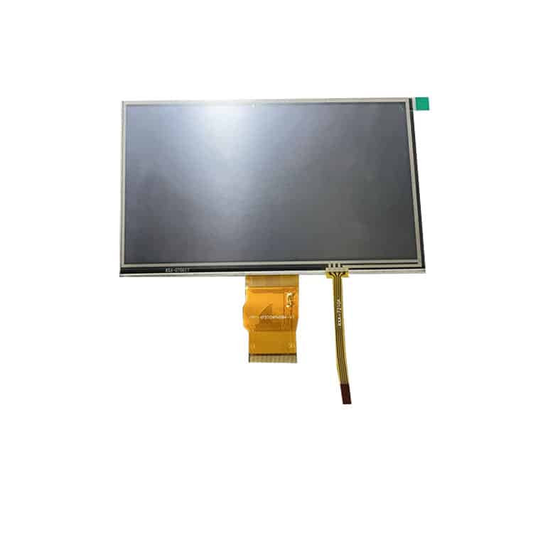
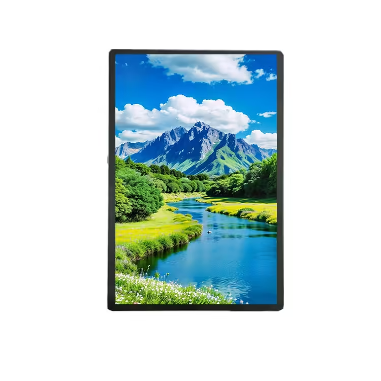
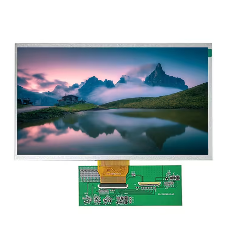
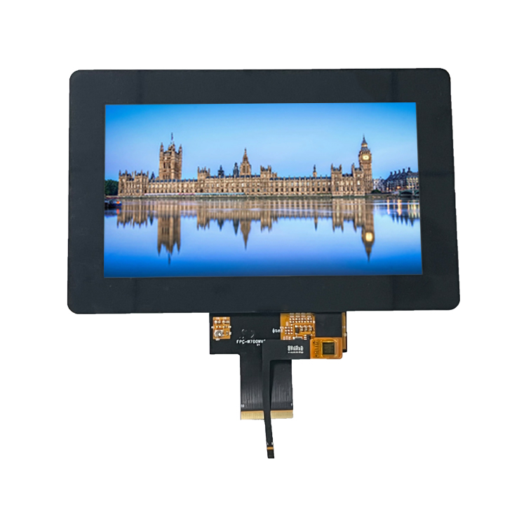
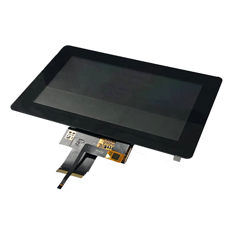
The FPC/Interface/luminance/Touch panel/Cover glass of our most products is customizable.
If you have any requirements, please contact us.
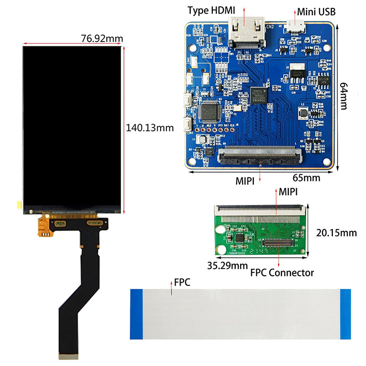
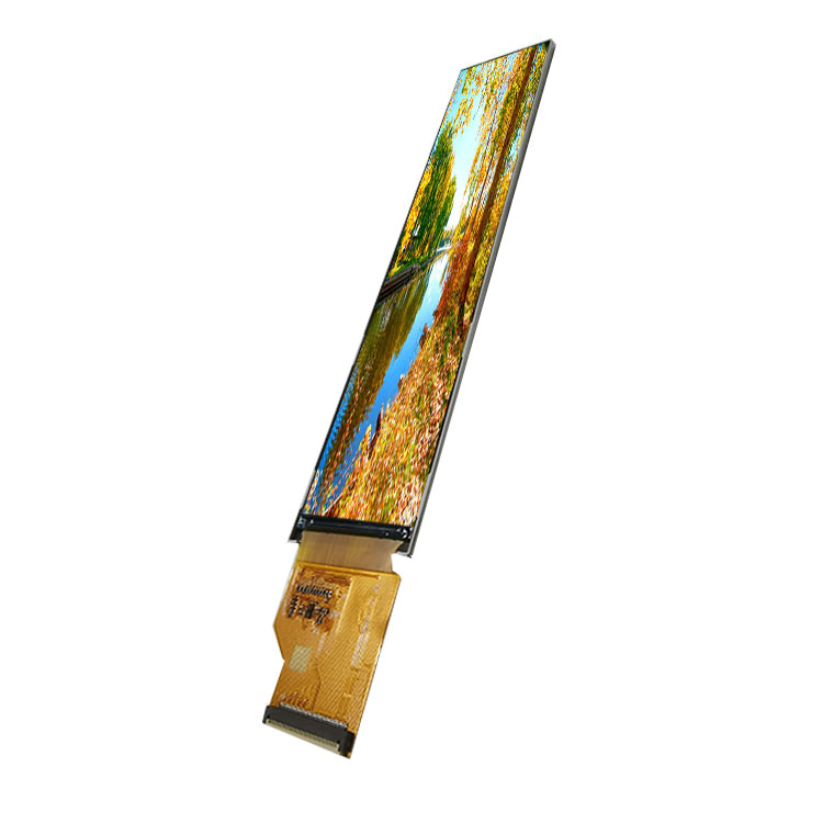
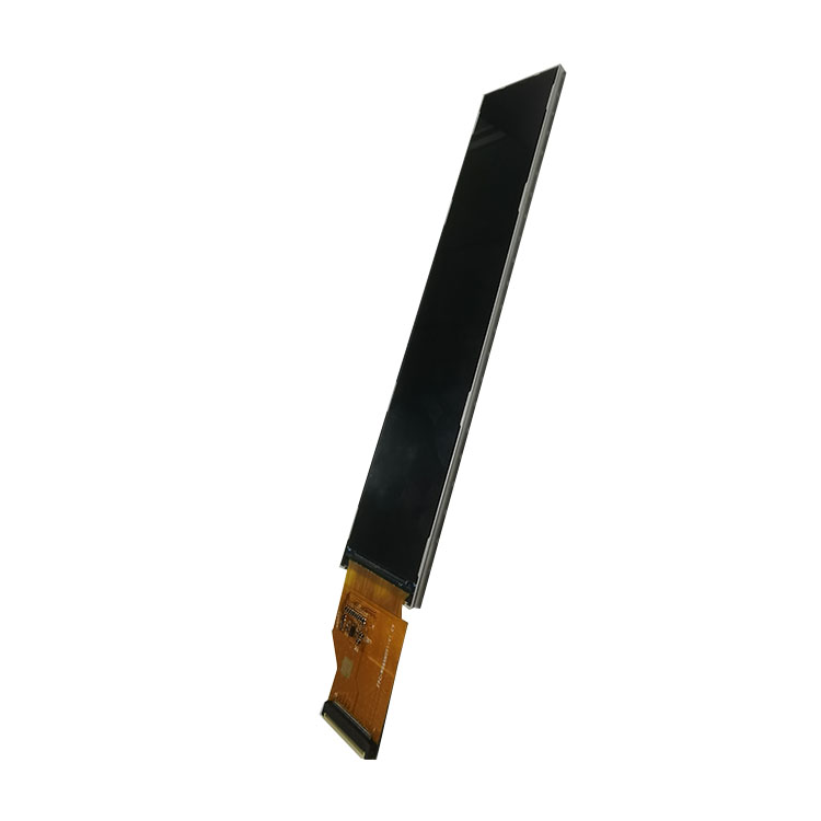
LS060R1SX02 is 5.98 inch tft lcd display module with MIPI interface and IPS All o’clock viewing angle screen. Customization is available. The shape is a rectangle with high resolution 1440*2560. Outline dimension is 76.92×140.13mm, thickness is 1.25 mm. Active area is 74.52 X 132.48 mm. This lcd display is coming out with 50 pins definition. Working temperature is -20 to +60℃, storage temperature is -30 to +70℃.
DRAWING

SPECIFICATIONS
| General Specification | |
|---|---|
| Part No. | LS060R1SX02 |
| LCM Outline Dimension(mm) | 76.92(W)×140.13 (H)×1.25(D) |
| Active Area(mm) | 74.52(H) X 132.48(V) |
| Number of Pixel(pixels) | 1440(H)×2560(V) |
| Display mode | New Mode2 |
| Operating temperature(°C) | -20 ~ 60℃ |
| Storage temperature(°C) | -30 ~ 70℃ |
| Interface | MIPI |
| Driver IC | R63419 |
| LCD Mode | Normally Black |
| Pixel Pitch(mm) | 0.01725(H) x 0.05175(V) |
| Viewing Direction | All o'clock |
| Pixel configuration | R,G,B vertical stripes |
| Pins Description | ||||
|---|---|---|---|---|
| PIN NO. | Symbol | Description | I/O | Remarks |
| 1 | GND | Ground | - | |
| 2 | DSI_A_D3N | MIPI data3 negative signal of MIPI Port A | I | |
| 3 | DSI_A_D3P | MIPI data3 positive signal of MIPI Port A | I | |
| 4 | GND | Ground | - | |
| 5 | DSI_A_CLKN | MIPI clock negative signal of MIPI Port A | I | |
| 6 | DSI A CLKP | MIPI clock positive signal of MIPI Port A | I | |
| 7 | GND | Ground | - | |
| 8 | DSI_A_D2N | MIPI data2 negative signal of MIPI Port A | I | |
| 9 | DSI A D2P | MIPI data2 positive signal of MIPI Port A | I | |
| 10 | GND | Ground | - | |
| 11 | DSI_B_D1P | MIPI data1 positive signal of MIPI Port B | I | |
| 12 | DSI_B_D1N | MIPI data1 negative signal of MIPI Port B | I | |
| 13 | GND | Ground | - | |
| 14 | DSI B DOP | MIPI data0 positive signal of MIPI Port B | I/O | |
| 15 | DSI_B_DON | MIPI dataO negative signal of MIPI Port B | I/O | |
| 16 | GND | Ground | - | |
| 17 | VSP | Power supply for analog positive | ||
| 18 | VSN | Power supply for analog negative | ||
| 19 | GND | Ground | - | |
| 20 | LEDK1 | LED cathode 1 | ||
| 21 | LEDK2 | LED cathode 2 | ||
| 22 | LEDK3(NC) | Non connect | ||
| 23 | LEDK4(NC) | Non connect | ||
| 24 | LEDA | LED anode | ||
| 25 | LEDA | LED anode | ||
| 26 | GND | Ground | - | |
| 27 | MIP | |||
| 28 | IOVCC | Power supply for I/O | - | |
| 29 | RESX | Reset enable pin | I | |
| 30 | IM | |||
| 31 | LCD_PWM | Backlight LED driver PWM | O | |
| 32 | TE | Tearing signal output from driver IC | O | |
| 33 | H-SYNC | Last data line STB of gate line period | O | |
| 34 | ID1 | ID Pin | ||
| 35 | GND | Ground | - | |
| 36 | DSI_B_D3N | MIPI Data3 negative of MIPI port B | I | |
| 37 | DSI_B_D3P | MIPI Data3 positive of MIPI port B | I | |
| 38 | GND | Ground | - | “L" Active |
| 39 | DSI_B_CLKN | MIPI clock negative signal of MIPI Port B | I | |
| 40 | DSI B CLKP | MIPI clock positive signal of MIPI Port B | I | |
| 41 | GND | Ground | - | |
| 42 | DSIB D2N | MIPI data2 negative signal of MIPI Port B | I | |
| 43 | DSIB D2P | MIPI data2 positive signal of MIPI Port B | I | |
| 44 | GND | Ground | - | |
| 45 | DSI_A_D1P | MIPI data1 positive signal of MIPI Port A | I | |
| 46 | DSI_A_D1N | MIPI data1 negative signal of MIPI Port A | I | |
| 47 | GND | Ground | - | |
| 48 | DSI A DOP | MIPI data0 positive signal of MIPI Port A | I/O | |
| 49 | DSI A DON | MIPI dataO negative signal of MIPI Port A | I/O | |
| 50 | GND | Ground | - | |


