


")
The FPC/Interface/luminance/Touch panel/Cover glass of our most products is customizable.
If you have any requirements, please contact us.
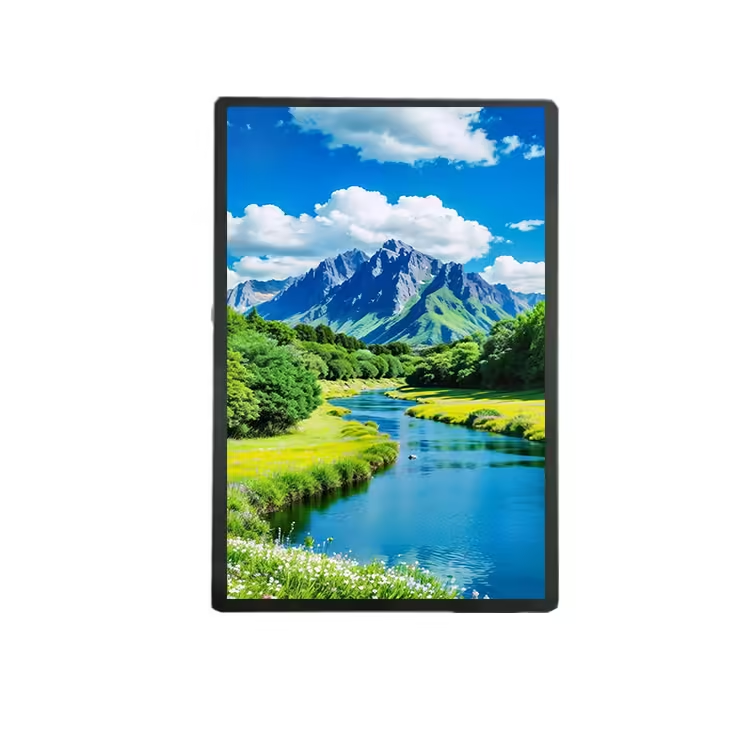
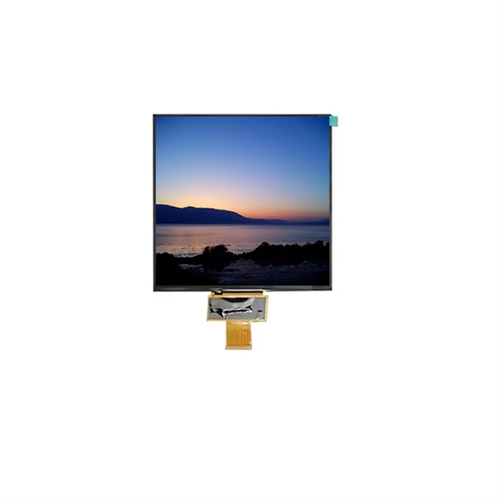
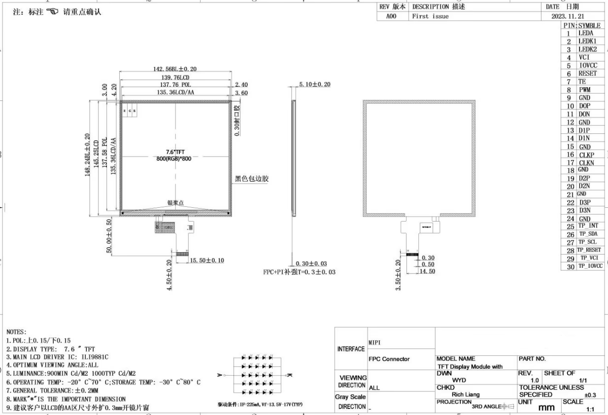
This 7.6-inch square TFT LCD features an 800×800 resolution, IPS technology for wide viewing angles, and 1000 nits brightness for excellent visibility. With a MIPI interface, it’s perfect for high-performance display applications.
DRAWING
SPECIFICATIONS
| General Specification | |
|---|---|
| Part No. | GX076-30MB-A1 |
| Supplier Type | Manufacturer |
| Place of Origin | Guangdong, China |
| Brand Name | Chance |
| Outline Dimension | 142.56 (H)*148.24 (V)*5.1(D) |
| Active Area | 135.36 (H)* 135.36 (V) |
| Pixel pitch | 36.5(H) x109.5(V) |
| Resolution | 800*800 |
| Interface | MIPI |
| Brightness | 1000cd/m2 |
| Colors | 16.7M |
| Viewing direction | Free |
| Operating Temperature | -20°C~ +70°C |
| Storage Temperature | -25°C~ +75°C |
| Module lifetime(Hours) | 50000 |
| Pin No. | Symbol | Description |
|---|---|---|
| 1 | LEDA | LED backlight anode. |
| 2 | LEDK | LED backlight cathode. |
| 3 | LEDK | LED backlight cathode. |
| 4 | VC I | Power supply for the an a log power |
| 5 | IOVCC | Power supply for the logic power and I/O circuit |
| 6 | RESET | Reset signal(low active) |
| 7 | TE | Tearing effect output |
| 8 | PWM | The PWM frequency output for LCD driver control. |
| 9 | GND | Power gro und |
| 10 | MIPI DP0 | MIPI-DSI data lane 0 posivtve input pin. |
| 11 | MIPI DN0 | MIPI-DSI data lane 0 negtive input pin. |
| 12 | GND | Power grou nd |
| 13 | MIPI DP1 | MIPI-DSI data lane 1 posivtve input pin. |
| 14 | MIPI DN1 | MIPI-DSI data lane 1 negtive input pin. |
| 15 | GND | Power grou nd |
| 16 | MIPI CLKP | MIPI-DSI data lane posivtve input pin. |
| 17 | MIPI CLKN | MIPI-DSI data lane negtive input pin. |
| 18 | GND | Power ground |
| 19 | MIPI DP2 | MIPI-DSI data lane 2 posivtve input pin. |
| 20 | MIPI DN2 | MIPI-DSI data lane 2 negtive input pin. |
| 21 | GND | Power grou nd |
| 22 | MIPI DP3 | MIPI-DSI data lane 3 posivtve input pin. |
| 23 | MIPI DN3 | MIPI-DSI data lane 3 negtive input pin. |
| 24 | GND | Power gro und |
| 25 | TP」NT | INT pin for CTP (NC) |
| 26 | TP SDA | SDA pin for CTP (NC) |
| 27 | TP SCL | SCL pin for CTP (NC) |
| 28 | TP RESET | Reset pinfo「TP (NC) |
| 29 | TP VCI | VCI pin for CTP (NC) |
| 30 | TP IOVCC | IOVCC pin for CTP (NC) |