The FPC/Interface/luminance/Touch panel/Cover glass of our most products is customizable.
If you have any requirements, please contact us.
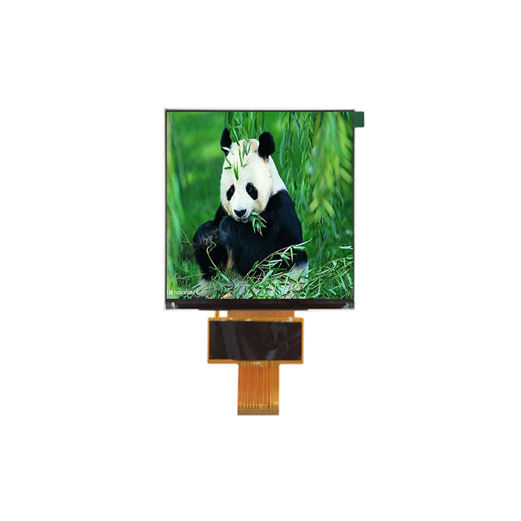
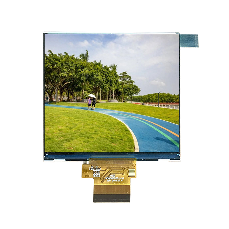
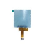
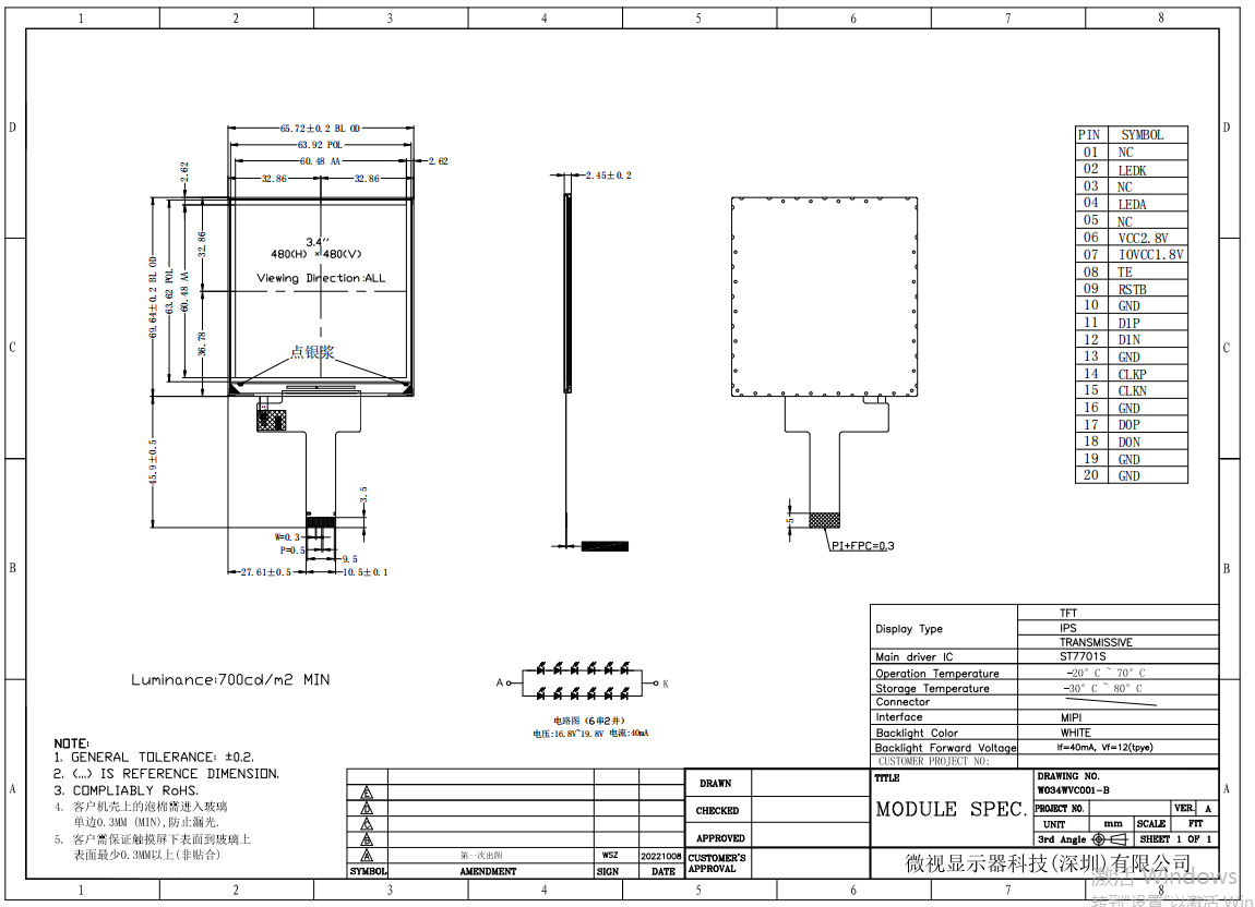
W034WVC001-B is 3.4 inch tft lcd display screen with MIPI interface with ips all viewing angle.Customization is available.The shape is a rectangle with resolution 480*480. Outline dimension is 65.72x 69.64mm, thickness is 2.45mm. Active area is 60.48×60.48mm. This lcd display is coming out with 20 pins defination. LCD driver IC is ST7701S, operating voltage is 2.5V~3.3V. Working temperature is -20 to 70℃, storage temperature is -30 to +80℃.
DRAWING
SPECIFICATIONS
| General Specification |
|
|---|---|
| Part No. | W034WVC001-B |
| LCM Outline Dimension(mm) | 65.72(H)X69.64(V)X2.45(T) |
| Active Area(mm) | 60.48 (H)X60.48 (V) |
| Number of Pixel(pixels) | 480(H)xRGBx480(V) |
| Touch panel | without |
| Operating temperature(°C) | -20 ~ 70℃ |
| Storage temperature(°C) | -30 ~ +80℃ |
| Driver IC | ST7701S |
| Brightness | 700 nits |
| Pixel Pitch | 0.042(H)×0.126(V) |
| Surface Treatment | Anti-Glare |
| Display mode | Normally Black,Transmissive |
| Interface | MIPI |
| Viewing Direction | All |
| Backlight | White LED |
| Module lifetime(Hours) | 50000 |
| Pins Description | ||||
|---|---|---|---|---|
| PIN NO. | Symbol | I/O or connect to | Description | When not in use |
| 1 | NC | - | No connect. | - |
| 2 | LEDK | LED DRIVER | This pin is used to be serial interface clock. | - |
| 3 | NC | - | No connect. | - |
| 4 | LEDA | LED DRIVER | Backlight anode. | - |
| 5 | NC | - | No connect. | - |
| 6 | VCC | PWR SUPPLY | Analog power supply, 2.5V~3.6V, type :2.8V . | - |
| 7 | IOVCC | PWR SUPPLY | Interface power supply, 1.65V ~ 3.6V, type: 1.8V. | - |
| 8 | TE | I/O | Tearing effect signal. | - |
| 9 | RESET | I/O | Reset pin. | - |
| 10 | GND | PWR SUPPLY | Power ground. | GND/IOVCC |
| 11 | D1P | I/O | Positive polarity of low voltage differential data signal. | - |
| 12 | D1N | I/O | Negaitive polarity of low voltage differential data signal. | GND/IOVCC |
| 13 | GND | PWR SUPPLY | Power ground. | GND/IOVCC |
| 14 | CLKP | I/O | Positive polarity of low voltage differential clock signal. | GND/IOVCC |
| 15 | CLKN | I/O | Negaitive polarity of low voltage differential clock signal. | GND/IOVCC |
| 16 | GND | PWR SUPPLY | Power ground. | - |
| 17 | D0P | I/O | Positive polarity of low voltage differential data signal. | - |
| 18 | D0N | I/O | Negaitive polarity of low voltage differential data signal. | GND/IOVCC |
| 19-20 | GND | PWR SUPPLY | Power ground. | GND/IOVCC |