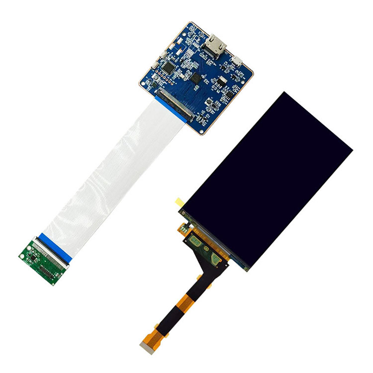
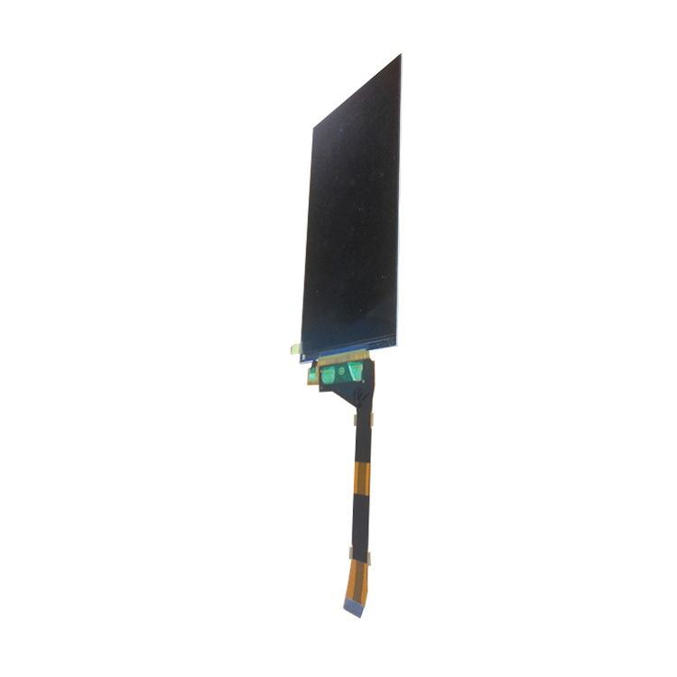
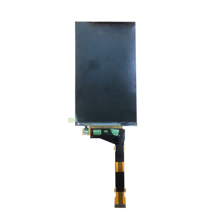
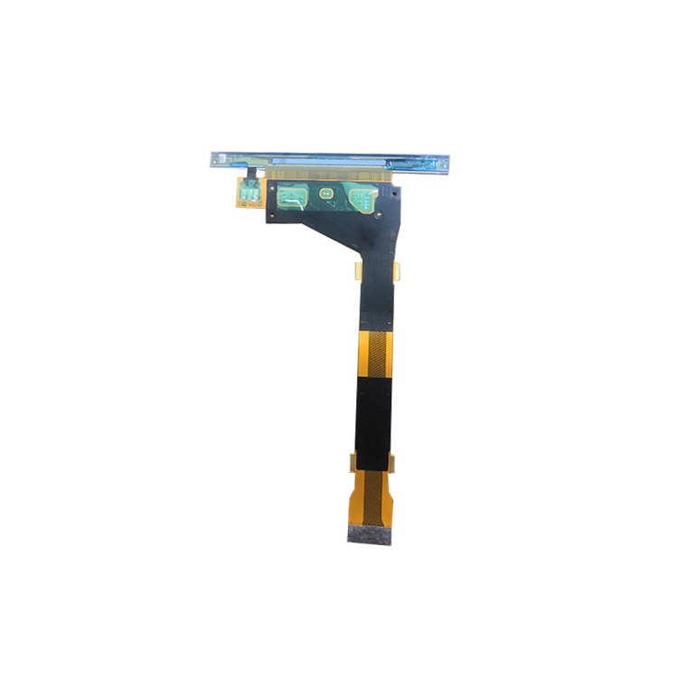
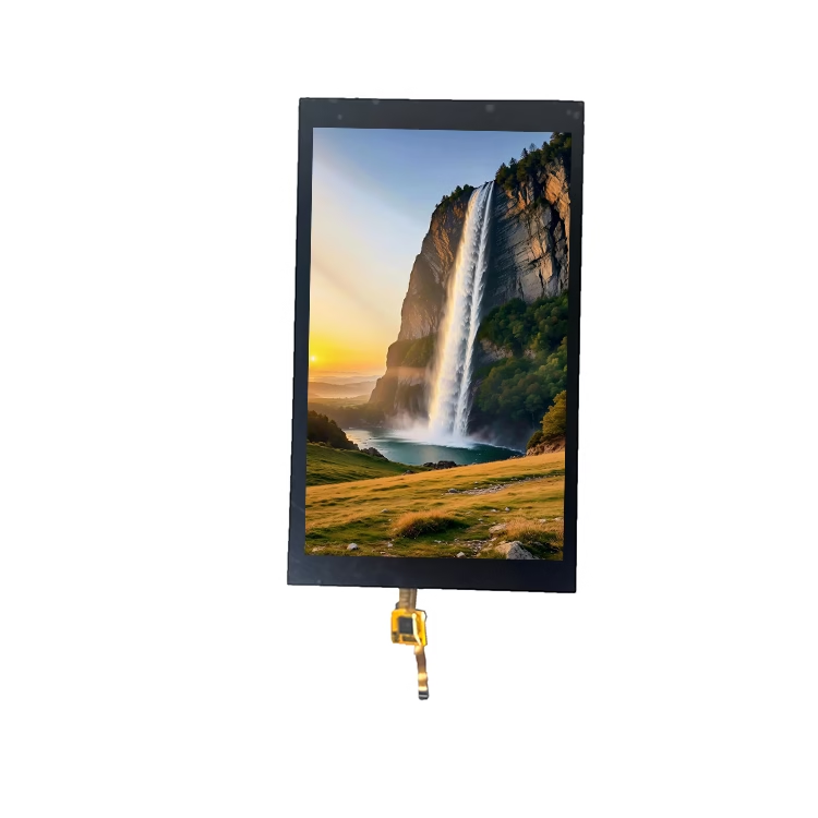
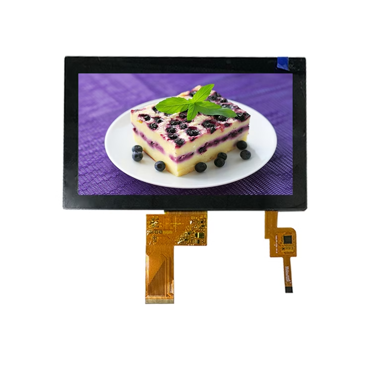
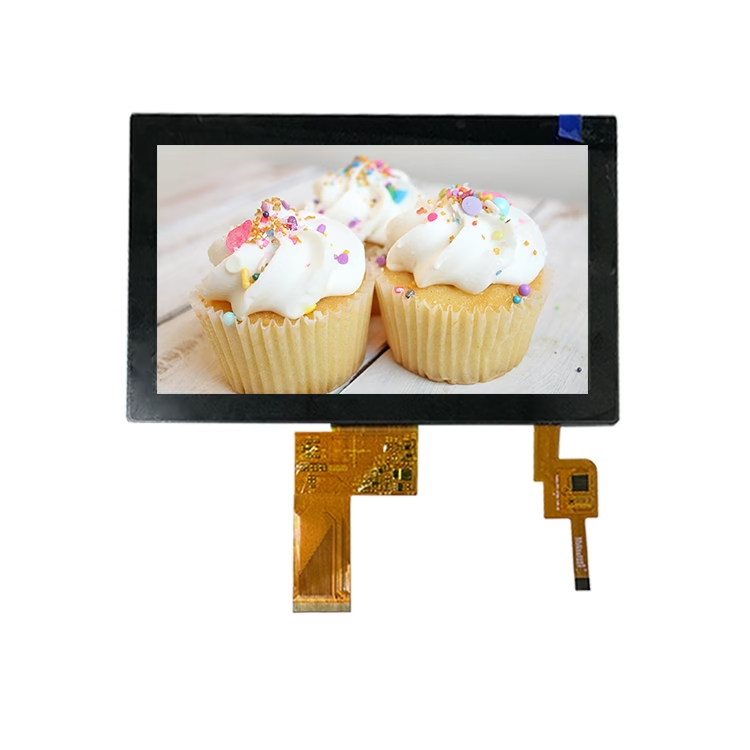
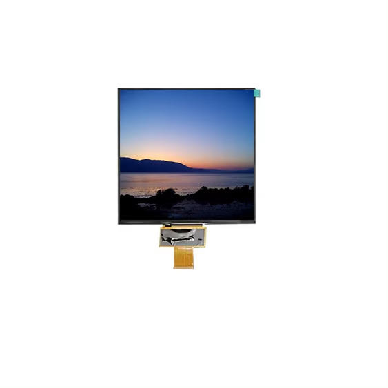
The FPC/Interface/luminance/Touch panel/Cover glass of our most products is customizable.
If you have any requirements, please contact us.
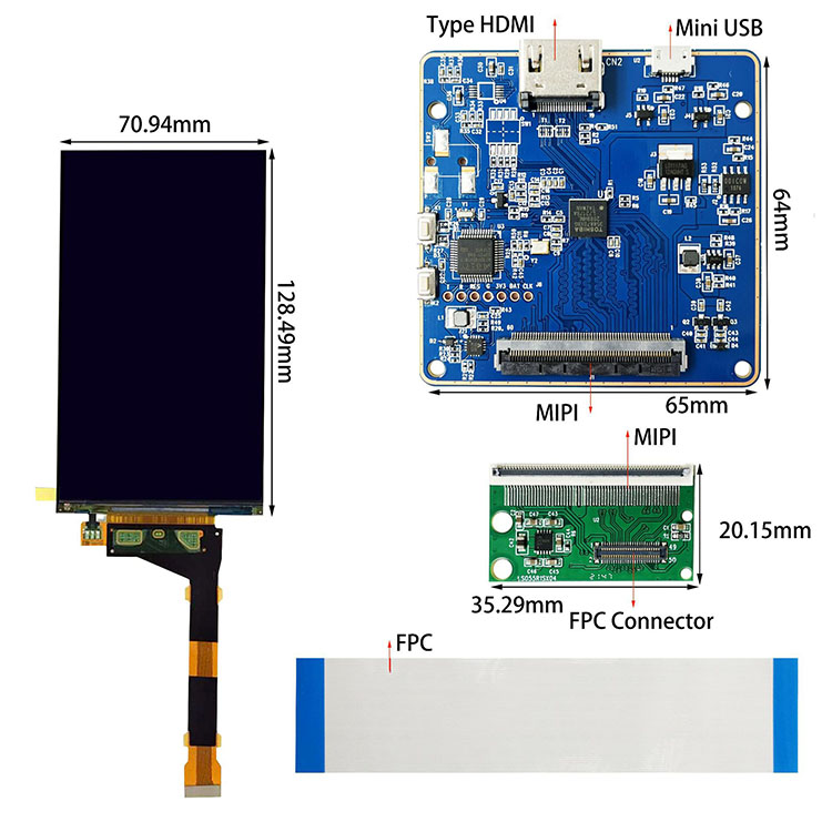
LS055R1SX04 is 5.46 inch tft lcd display module with MIPI interface and IPS All o’clock viewing angle screen. Customization is available. The shape is a rectangle with high resolution 1440*2560. Outline dimension is 70.94×128.49mm, thickness is 1.35 mm. Active area is 68.04X120.96 mm. This lcd display is coming out with 50 pins definition. Working temperature is -20 to +60℃, storage temperature is -30 to +70℃.
DRAWING

SPECIFICATIONS
| General Specification | |
|---|---|
| Part No. | LS055R1SX04 |
| LCM Outline Dimension(mm) | 70.94(W)×128.49 (H)×1.35(D) |
| Active Area(mm) | 68.04(H)X120.96(V) |
| Number of Pixel(pixels) | 1440(H)×2560(V) |
| Display mode | New Mode2 |
| Operating temperature(°C) | -20 ~ 60℃ |
| Storage temperature(°C) | -30 ~ 70℃ |
| Interface | MIPI |
| Driver IC | R63419 |
| LCD Mode | Normally Black |
| Pixel Pitch(mm) | 0.01575(H) x 0.04725(V) |
| Viewing Direction | All o'clock |
| Pixel configuration | R,G,B vertical stripes |
| Pins Description | ||||
|---|---|---|---|---|
| PIN NO. | Symbol | Description | I/O | Remarks |
| 1 | GND | Ground | - | |
| 2 | GND | Ground | - | |
| 3 | VSN | Power supply for analog(-5.75V) | - | |
| 4 | VSP | Power supply for analog(+5.75V) | - | |
| 5 | HSYNC | Horizontal Synchronizing signal | O | |
| 6 | GND | Ground | - | |
| 7 | GND | Ground | - | |
| 8 | DSI_A_D3- | MIPI DSI(-) of Port A | I | |
| 9 | DSI_A_D0- | MIPI DSI(-)of Port A | I/O | |
| 10 | DSI_A_D3+ | MIPI DSI(+) of Port A | I | |
| 11 | DSI_A_D0+ | MIPI DSI(+) of Port A | I/O | |
| 12 | GND | Ground | - | |
| 13 | GND | Ground | - | |
| 14 | DSI A CLK- | MIPI DSI Clock(-) of PortA | I | |
| 15 | DSI_A_D1- | MIPI DSI (-) of PortA | I | |
| 16 | DSI_A_CLK+ | MIPI DSI Clock(+) of PortA | I | |
| 17 | DSI_A_D1+ | MIPI DSI(+) of PortA | I | |
| 18 | GND | Ground | - | |
| 19 | GND | Ground | - | |
| 20 | DSI_A_D2- | MIPI DSI (-) of PortA | I | |
| 21 | DSI_B_D2+ | MIPI DSI (+) of PortB | I | |
| 22 | DSI A D2+ | MIPI DSI(+) of PortA | I | |
| 23 | DSI_B_D2- | MIPI DSI (-)of PortB | I | |
| 24 | GND | Ground | - | |
| 25 | GND | Ground | - | |
| 26 | DSI_B_D1+ | MIPI DSI(+) of PortB | I | |
| 27 | DSI_B_CLK+ | MIPI DSI Clock (+) of PortB | I | |
| 28 | DSI_B_D1- | MIPI DSI (-)of PortB | I | |
| 29 | DSI_B_CLK- | MIPI DSI Clock(-) of PortB | I | |
| 30 | GND | Ground | - | |
| 31 | GND | Ground | - | |
| 32 | DSI_B_D0+ | MIPI DSI (+) of PortB | I/O | |
| 33 | DSI_B_D3+ | MIPI DSI (+) of PortB | I | |
| 34 | DSI_B_D0- | MIPI DSI(-) of PortB | I/O | |
| 35 | DSI_B_D3- | MIPI DSI (-)of PortB | I | |
| 36 | GND | Ground | - | |
| 37 | GND | Ground | - | |
| 38 | RESX | Device reset signal | I | “L" Active |
| 39 | IOVCC | Power supply for I/O | - | |
| 40 | TE | Tearing signal output from driver IC | O | |
| 41 | IOVCC | Power supply for I/O | - | |
| 42 | GND | Ground | - | |
| 43 | GND | Ground | - | |
| 44 | LED_PWM | Control signal for brightness of LED backlight | O | |
| 45 | ID1 | ID1(connect to VDDI in FPC) | - | |
| 46 | ID2 | ID2(connect to VDDI in FPC) | - | |
| 47 | LED1- | LED back light power negative1 (group1) | ||
| 48 | LED+ | LED back light power positive | - | |
| 49 | LED2- | LED back light power negative1(group2) | ||
| 50 | NC | No connect | - | |


