


The FPC/Interface/luminance/Touch panel/Cover glass of our most products is customizable.
If you have any requirements, please contact us.
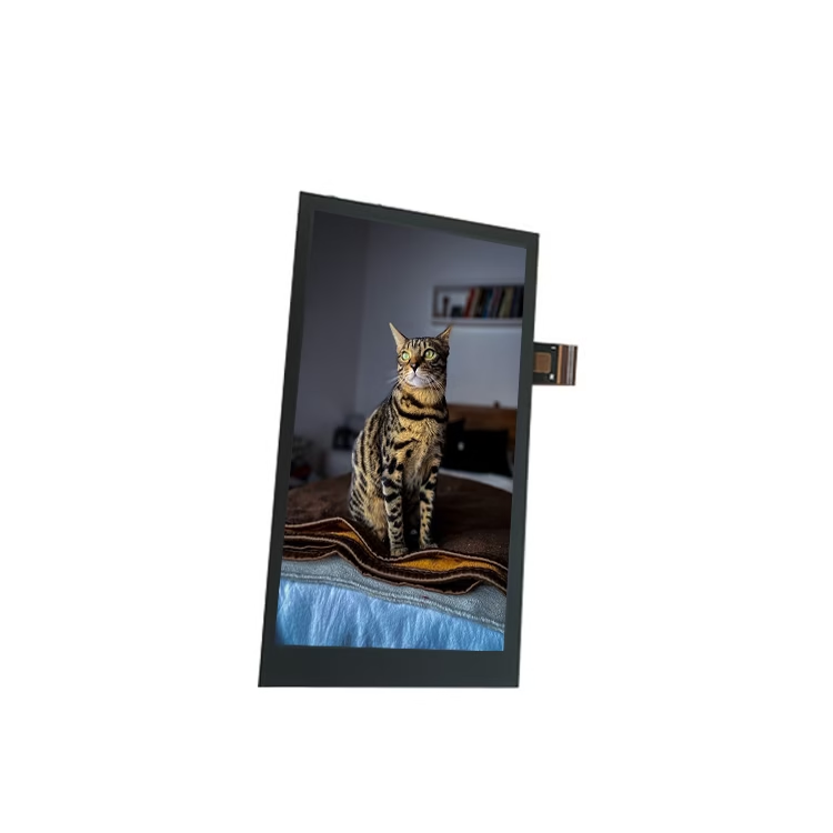
W550FHC010-A-CT is a color active matrix LCD module incorporating amorphous silicon TFT(Thin Film Transistor). It is composed of a color TFT-LCD panel, driver ICs, FPC, and a backlight unit. The 5.5′′ display area contains 1080 (RGB) x 1920 pixels and can display up to 262K colors.
DRAWING

SPECIFICATIONS
| General Specification | |
|---|---|
| Part No. | W550FHC010-A-CT |
| Display Mode | Normally Blackjransmissive |
| Display Technology | a-Si TFT active matrix |
| Outline Dimension | 76.44(H) X 135.20(V) X 3.05(T) |
| Active Area | 68.04 (H)X 120.96 (V) |
| Resolution | 1080 X(RGB) X1920 |
| Pixel Pitch | 21(H)x63(V) |
| Backlight | White LED |
| Luminance | 1000 |
| Surface Treatme nt | Anti-Glare |
| Driver IC | HX8399C |
| Viewing Direction | FREE |
| Module lifetime(Hours) | 50000 |
| PIN NO | Symbol | I/O or connect to | Desaiption |
|---|---|---|---|
| 1 | VDD | PWR SUPPLY | Analog power supply, 2.5V~3.6V. type : 2.8V . |
| 2 | IOVCC | PWR SUPPLY | Interface power supply, 1.65V ~ 3.6V. type: 1.8V. |
| 3 | NC | - | No connect |
| 4 | TE | I/O | Tearing effect signal. |
| 5 | RESET | I/O | Reset pin. |
| 6 | GND | PWR SUPPLY | Power ground. |
| 7 | D3P | I/O | Positive polarity of low voltage differential data3 signal. |
| 8 | D3N | I/O | Negaitive polarity of low voltage differential data3 signal. |
| 9 | GND | PWR SUPPLY | Power grou nd. |
| 10 | D2N | I/O | Negaitive polarity of low voltage differential data2 signal. |
| 11 | D2P | I/O | Positive polarity of low voltage differential data2 signal. |
| 12 | GND | PWR SUPPLY | Power ground. |
| 13 | DIP | I/O | Positive polarity of low voltage differential datal signal. |
| 14 | DIN | I/O | Negaitive polarity of low voltage differential datal signal. |
| 15 | GND | PWR SUPPLY | Power ground. |
| 16 | DON | I/O | Negaitive polarity of low voltage differential dataO signal. |
| 17 | DOP | I/O | Positive polarity of low voltage differential dataO signal. |
| 18 | GND | PWR SUPPLY | Power ground. |
| 19 | CLKP | I/O | Positive polarity of low voltage differential dock signal. |
| 20 | CLKN | I/O | Negaitive polarity of low voltage differential clock signal. |
| 21 | GND | PWR SUPPLY | Power ground. |
| 22 | CTP-RST | CTP Reset pin | |
| 23 | CTP-SDA | CTP data input. | |
| 24 | CTP-SCL | CTP dock pulses | |
| 25 | CTP-INT | CTP interrupt signa | |
| 26 | CTP-VDD | CTP Analog power supply, 2.8v | |
| 27 | GND | PWR SUPPLY | Power ground. |
| 28-30 | NC | - | No connect |
| 31-33 | LED+ | LED DRIVER | Backlight anode. |
| 34-36 | NC | - | No connect |
| 37-39 | LED- | l ED DRIVER | This pin is used to be serial interface clock・ |