


The FPC/Interface/luminance/Touch panel/Cover glass of our most products is customizable.
If you have any requirements, please contact us.
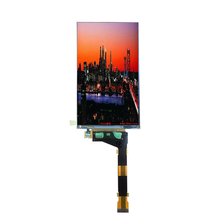
The LS054B3SX01(G) is a 5.36/5.4-inch high-resolution IPS LCD screen with a stunning 1152×1920 resolution. Featuring an IPS panel, it offers exceptional color accuracy and wide viewing angles, making it ideal for devices requiring superior display quality. Equipped with a MIPI interface, it ensures fast and reliable communication with modern electronics.
DRAWING

SPECIFICATIONS
| Description | |
|---|---|
| Supplier Type | Manufacturer |
| Place of Origin | Guangdong, China |
| Brand Name | Chance |
| Type | TFT |
| Brand Name | Chance |
| Interface | MIPI |
| Viewing Angle | All O'clock |
| Outline Dimension | 72.00(W)*123.4 (H)*1.27(D) mm |
| Pixel configuration | R,G,B vertical stripes |
| Mass | Approx 25 g |
| Display mode | Normal Black |
| Active Area | 69.984(W)*116.64(H) |
| Model NO | LS054B3SX01(G) |
| Pin No | Svmbol | Description | I/O | Remarks |
|---|---|---|---|---|
| I | LED1+ | Power supply for LED (Anode) | I | |
| 2 | GND | GND level pin | - | |
| 3 | LED2+ | Power supply tor LED (Anode) | I | |
| 4 | D3 N | MIPI-DS1 Data diftereniiai input pins.(Dala Iane3) | I | |
| 5 | LED2- | Power supply lor LED (Cathode) | I | |
| 6 | D3 P | Ml PI-DS 1 Data difierential inpul pins.( Data Ianc3) | I | |
| 7 | LEDI・ | Power supply for LED (Cathode) | I | |
| 8 9 | GND VGL | GND level pin 3powcr:IC internal output signal 5oovver: Power suddIv tor LCD | - | 3power:For user, please open 5oower:VGL=-6.95±0.15V |
| 10 | D0 N | MIPI-DSI Data differential input pins.(Data land)) | I/O | |
| 11 | GND | GND level pin | - | |
| 12 | D0 P | MIPI-DSI Data differential inpul pins.(Daia land)) | I/O | |
| 13 | VSP | Power supply for LCD | I | VSP=5.7±0.15V |
| 14 | GND | GND level pin | - | |
| 15 | VSN | Power supply for LCD | I | VSN=・5.7±O.15V |
| 16 | CLK N | MIPI-DSI Clock difierential inpul pins. | I | |
| 17 | IOVCC | Power supply for LCD | I | IOVCC=1.8±0.15V |
| 18 | CLK P | MIPI-DSI Clock difierential input pins. | I | |
| 19 | LCDJD | Supplier information terminal (VDD level) | O | (SHARP: Connect to IOVCC) |
| 20 | GND | GND level pin | - | |
| 21 | GND | GND level pin | - | |
| 22 | D1 N | MIPI-DSI Data difierential input pins.(Data lanel) | I | |
| 23 | RESET | H/W Reset pin | I | |
| 24 | D1 P | MIPI-DSI Data diftereniiai inpul pins.(Da【a lanel) | I | |
| 25 | TE | Internal VSYNC output (use TP control) | O | |
| 26 | GND | GND level pin | - | |
| 27 | TE1 | Iniemal HSYNC output (use TP control) | O | |
| 28 | D2 N | MIPI-DSI Data difierential input pi ns .(Data Iane2) | I | |
| 29 | PWM | Backlight brightness control pin | O | |
| 30 | D2 P | MIPI-DSI Data differential inpul pins.(Data lane2) | I | |
| 31 | VGH | 3powcr:IC internal output signal 5power: Power supply for LCD | - | 3povver:For user, please open 5power:VGH=9.55± 0.15V |
| 32 | GND | GND level pin | - |