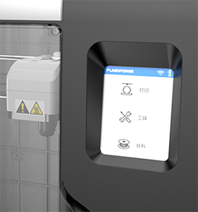
The FPC/Interface/luminance/Touch panel/Cover glass of our most products is customizable.
If you have any requirements, please contact us.
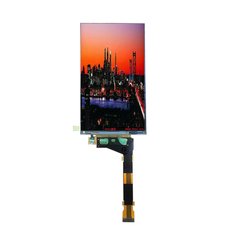
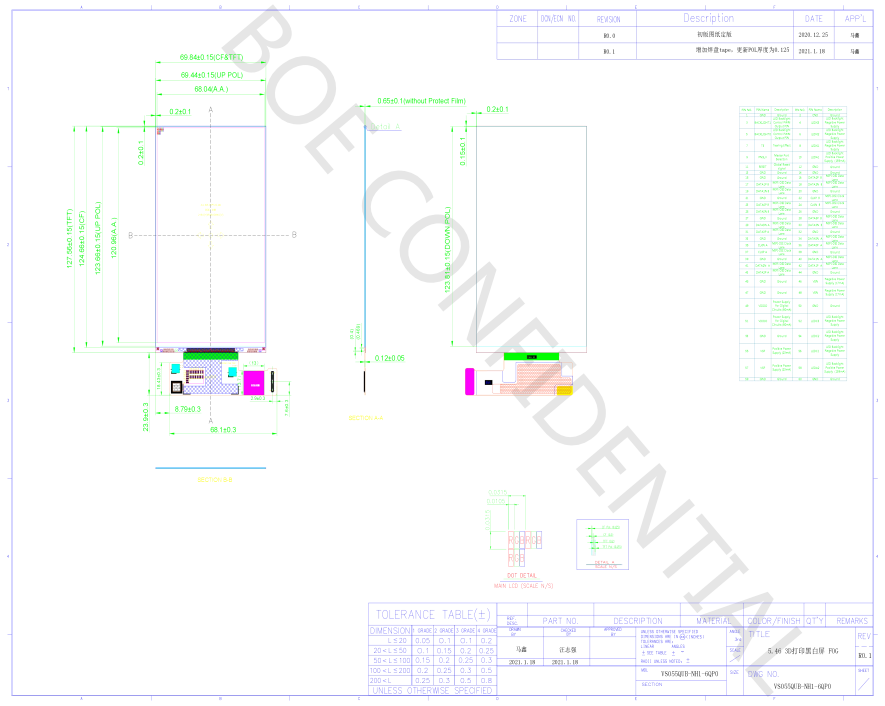
VS055QUB-NH1-DQP0 is 5.5 inch ips all viewing angle tft lcd display screen with MIPI interface.Customization is available.The resolution is 2160*3840. FOG Outline dimension is 69.82×127.56mm, thickness is 0.95mm. Active area is 68.04×120.96mm. This lcd display is coming out with 60 pins defination. LCD driver IC is R63455.Working temperature is 0 to 60℃, storage temperature is -10 to +70℃.
DRAWING
SPECIFICATIONS
| General Specification | |
|---|---|
| Part No. | VS055QUB-NH1-DQP0 |
| FOG Outline Dimension(mm) | 68.04(H) X 120.96(V) X 0.65(T) |
| Active Area(mm) | 68.04 (H) X 120.96(V) |
| Number of Pixel(pixels) | 2160X(RGB)X3840 |
| Touch panel | without |
| Operating temperature(°C) | 0 ~ +60℃ |
| Storage temperature(°C) | -10 ~ +70℃ |
| Driver IC | R63455 |
| Pixel Pitch | 0.0105(H)×0.0315(V) |
| Interface | MIPI 4 Lane*2 |
| Viewing Direction | All o'clock |
| Pixel Arrangement | stripe |
| LCM Weight(gram) | 13.9±2.0 |
| Display Method | Active Matrix TFT |
| Display Mode | Transmission Mode,Normally black |
| Pins Description | ||
|---|---|---|
| PIN NO. | Symbol | Description |
| 1 | GND | Ground |
| 2 | CND | Ground |
| 3 | BACKLIGHT1 | LED Backlight Control PWM Output PIN |
| 4 | LEDK3 | LED Backlight Negative Power Supply |
| 5 | BACKLIGHTO | LED Backlight Control PWM Output PIN |
| 6 | LEDK2 | LED Backlight Negative Power Supply |
| 7 | TE | Tearing Effect |
| 8 | LEDK1 | LED Backlight Negative Power Supply |
| 9 | PNSLV | Ground |
| 10 | LEDA1 | LED Backlight Positive Power Supply |
| 11 | RESET | Global Reset signal |
| 12 | GND | Ground |
| 13 | GND | Ground |
| 14 | GND | Ground |
| 15 | GND | Ground |
| 16 | DATA2P B | MIPJ-DSI Data Lane |
| 17 | DATA1P B | MIPI-DSI Data Lane |
| 18 | DATA2N B | MIPI-DSI Data Lane |
| 19 | DATA1N B | MIPI-DSI Data Lane |
| 20 | GND | Ground |
| 21 | GND | Ground |
| 22 | CLKP B | MIPI-DSI Clock Lane |
| 23 | DATAOP B | MIPI-DSI Data Lane |
| 24 | CLKN B | MIPI-DSI Clock Lane |
| 25 | DATA0N B | MIPI-DSI Data Lane |
| 26 | GND | Ground |
| 27 | GND | Ground |
| 28 | DATA3P B | MIPI-DSI Data Lane |
| 29 | DATA3N A | MIPI-DSI Data Lane |
| 30 | DATA3N B | MIPI-DSI Data Lane |
| 31 | DATA3P A | MIPI-DSI Data Lane |
| 32 | GND | Ground |
| 33 | GND | Ground |
| 34 | DATAON A | MIPI-DSI Data Lane |
| 35 | CLKN A | MIPI-DSI Clock Lane |
| 36 | DATAOP A | MIPI-DSI Data Lane |
| 37 | CLKP A | MIPI-DSI Clock Lane |
| 38 | GND | Ground |
| 39 | GND | Ground |
| 40 | DATA1N A | MIPI-DSI Data Lane |
| 41 | DATA2N A | MIPI-DSI Data Lane |
| 42 | DATA1P A | MIPI-DSI Data Lane |
| 43 | DATA2P A | MIPI-DSI Data Lane |
| 44 | GND | Ground |
| 45 | GND | Ground |
| 46 | VSN | Negative Power Supply |
| 47 | GND | Ground |
| 48 | VSN | Negative Power Supply |
| 49 | VDDIO | Power Supply For Digital Circuits |
| 50 | GND | Ground |
| 51 | VDDIO | Power Supply For Digital Circuits |
| 52 | LEDC3 | LED Backlight Negative Power Supply |
| 53 | GND | Ground |
| 54 | LEDC2 | LED Backlight Negative Power Supply |
| 55 | VSP | Positive Power Supply |
| 56 | LEDC1 | LED Backlight Negative Power Supply |
| 57 | VSP | Positive Power Supply |
| 58 | LEDA2 | LED Backlight Positive Power Supply |
| 59 | GND | Ground |
| 60 | GND | Ground |