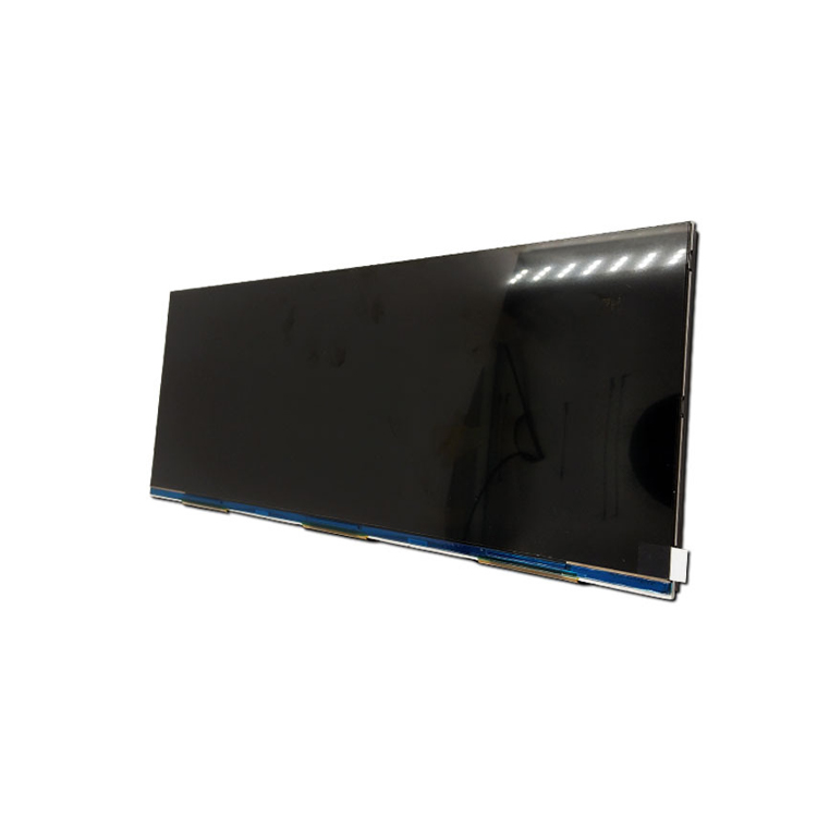
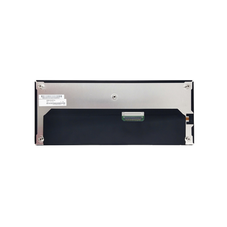
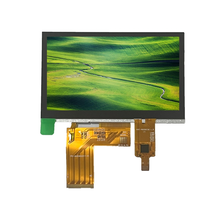
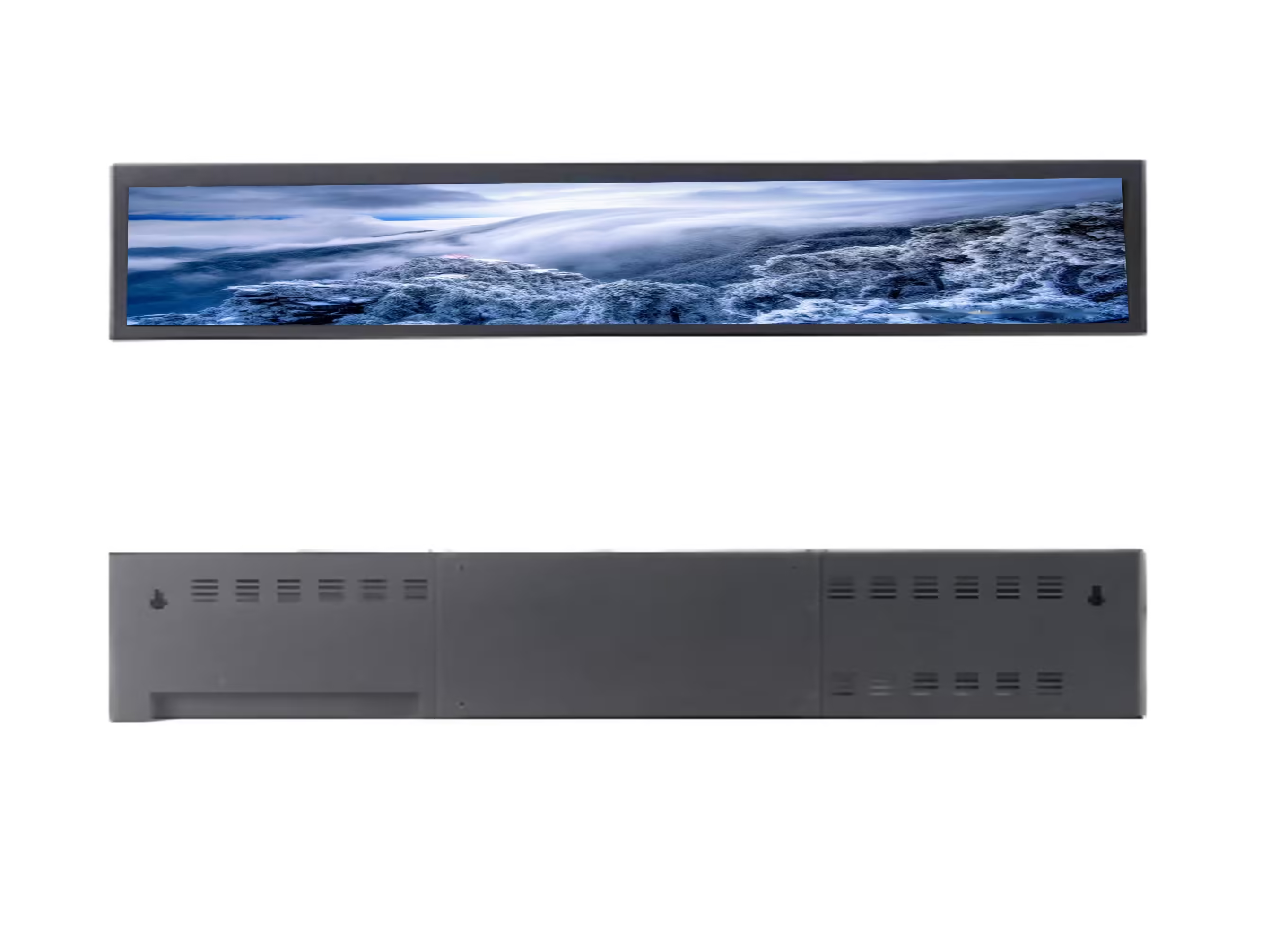
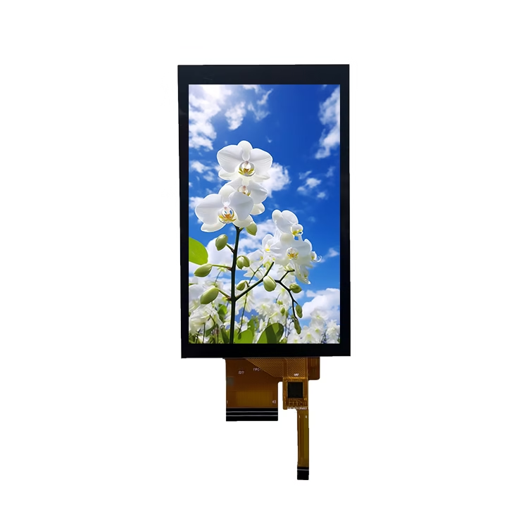
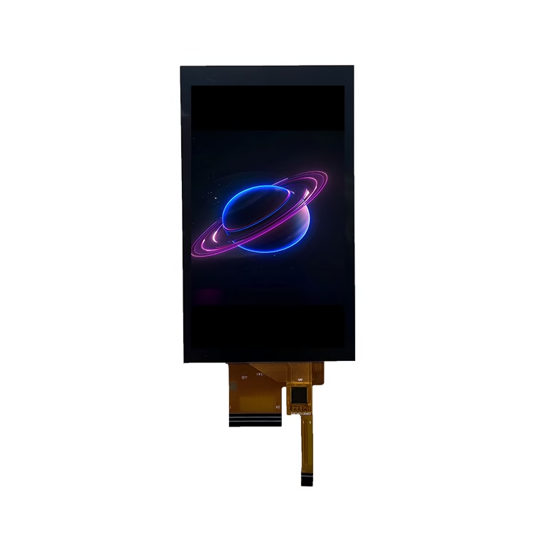
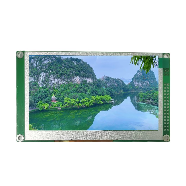
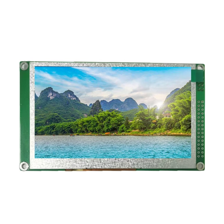
The FPC/Interface/luminance/Touch panel/Cover glass of our most products is customizable.
If you have any requirements, please contact us.
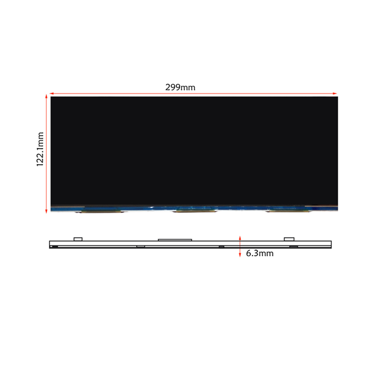
HSD123JPW4 is 12.3 inch all o’clock viewing angle tft lcd display screen with resolution 1920*720. Outline dimension is 299×122.1mm, thickness is 5.6mm. Active area is 292.032×109.512mm. This lcd display is coming out with 60 pins defination. Operating voltage is 3.0V~3.6V. Working temperature is -30 to +85℃, storage temperature is -40 to +90℃.
DRAWING

SPECIFICATIONS
| General Specification | |
|---|---|
| Part No. | HSD123JPW4 |
| LCM Outline Dimension(mm) | 299(H)X122.1(V)X5.6(T) |
| Active Area(mm) | 292.032(H)X109.512(V) |
| Number of Pixel(pixels) | 1920X(RGB)X720 |
| Touch panel | without |
| Operating temperature(°C) | -30 ~ +85℃ |
| Storage temperature(°C) | -40 ~ +90℃ |
| Brightness | 850nits |
| Pixel arrangement | RGB Vertical stripe |
| Display mode | Normally Black,Transmissive |
| Viewing Direction | All o'clock |
| Surface treatment | HC (Glare) |
| Weight | 395g |
| Backlight | Single LED (Side-Light type) |
| Power Consumption | 10.404W |
| Module lifetime(Hours) | 50000 |
| Pins Description | ||
|---|---|---|
| PIN NO. | Symbol | Description |
| 1 | GND | Power Ground |
| 2 | NC | No connector |
| 3 | VCC | Digital Power |
| 4 | VCC | Digital Power |
| 5 | GND | Power Ground |
| 6 | GND | Power Ground |
| 7 | PVPP | OTP power |
| 8 | NC | No connector |
| 9 | GND | Power Ground |
| 10 | ORXIN0- | Odd pixel negative LVDS differential clock input |
| 11 | ORXIN0+ | Odd pixel positive LVDS differential clock input |
| 12 | ORXIN1- | Odd pixel negative LVDS differential clock input |
| 13 | ORXIN1+ | Odd pixel positive LVDS differential clock input |
| 14 | ORXIN2- | Odd pixel negative LVDS differential clock input |
| 15 | ORXIN2+ | Odd pixel positive LVDS differential clock input |
| 16 | ORXCLKIN- | Odd pixel negative LVDS differential clock input |
| 17 | ORXCLKIN+ | Odd pixel positive LVDS differential clock input |
| 18 | ORXIN3- | Odd pixel negative LVDS differential clock input |
| 19 | ORXIN3+ | Odd pixel positive LVDS differential clock input |
| 20 | ERXIN0- | Even pixel negative LVDS differential clock input |
| 21 | ERXIN0+ | Even pixel positive LVDS differential clock input |
| 22 | ERXIN1- | Even pixel negative LVDS differential clock input |
| 23 | ERXIN1+ | Even pixel positive LVDS differential clock input |
| 24 | ERXIN2- | Even pixel negative LVDS differential clock input |
| 25 | ERXIN2+ | Even pixel positive LVDS differential clock input |
| 26 | ERXCLKIN- | Even pixel negative LVDS differential clock input |
| 27 | ERXCLKIN+ | Even pixel positive LVDS differential clock input |
| 28 | ERXIN3- | Even pixel negative LVDS differential clock input |
| 29 | ERXIN3+ | Even pixel positive LVDS differential clock input |
| 30 | GND | Power Ground |
| 31 | NC | No connector |
| 32 | RESETB | RESETB Global reset pin,active low. |
| 33 | NC | No connector |
| 34 | SCL | Serial interface clock input. |
| 35 | SDA | Serial interface data input/output. |
| 36 | CSX | Serial interface chip enable. |
| 37 | SDO | Serial interface output pin. |
| 38 | Fail _DET | Fail _DET |
| 39 | GND | Power Ground |
| 40 | GND | Power Ground |
| 41 | NC | No connector |
| 42 | TP_EXT_RSTN | TP external reset signal |
| 43 | TSIX | TouchScreen interrupt line |
| 44 | TP_SPI_MOSI | SPI Slave interface input pin for touch |
| 45 | TP_SPI_MISO | SPI Slave interface output pin for touch |
| 46 | TP_SPI_SCL | SPI slave clock input for touch |
| 47 | TP_SS | SPI slave chip select input for touch |
| 48 | TP_GPIO[0] | Programmable I/Opins. |
| 49 | NC | No connector |
| 50 | LEDA | LED power (Anode) |
| 51 | LEDA | LED power (Anode) |
| 52 | LEDA | LED power (Anode) |
| 53 | NC | No connector |
| 54 | LEDK1 | Cathode 1 |
| 55 | LEDK2 | Cathode 2 |
| 56 | LEDK3 | Cathode 3 |
| 57 | LEDK4 | Cathode 4 |
| 58 | NTC_A | NTC_Anode |
| 59 | NTC_K | NTC_Cathode |
| 60 | GND | Power Ground |


