


The FPC/Interface/luminance/Touch panel/Cover glass of our most products is customizable.
If you have any requirements, please contact us.
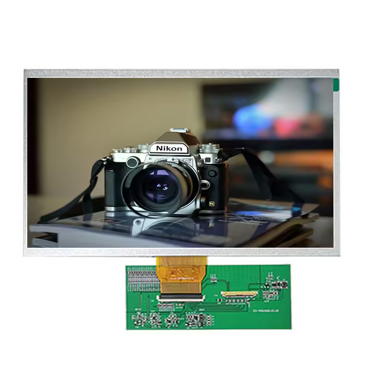
The 8-inch IPS TFT LCD Display with a 1024×768 resolution and LVDS interface combines outstanding image quality and a wide viewing angle for clear and vibrant visuals. This TFT LCD module is designed to provide reliable performance and excellent color reproduction, making it ideal for diverse applications.
DRAWING

SPECIFICATIONS
| General Specification | |
|---|---|
| Part No. | CH-080H001 |
| LCD size | 8.0 inch(Diagonal) |
| Driver eleme nt | a-Si TFT active matrix |
| Resolution | 1024 X 3(RGB) X 768 |
| Display mode | Normally Black, Transmissive |
| Dot pitch | 0.05275(W) X 0.15825(H) mm |
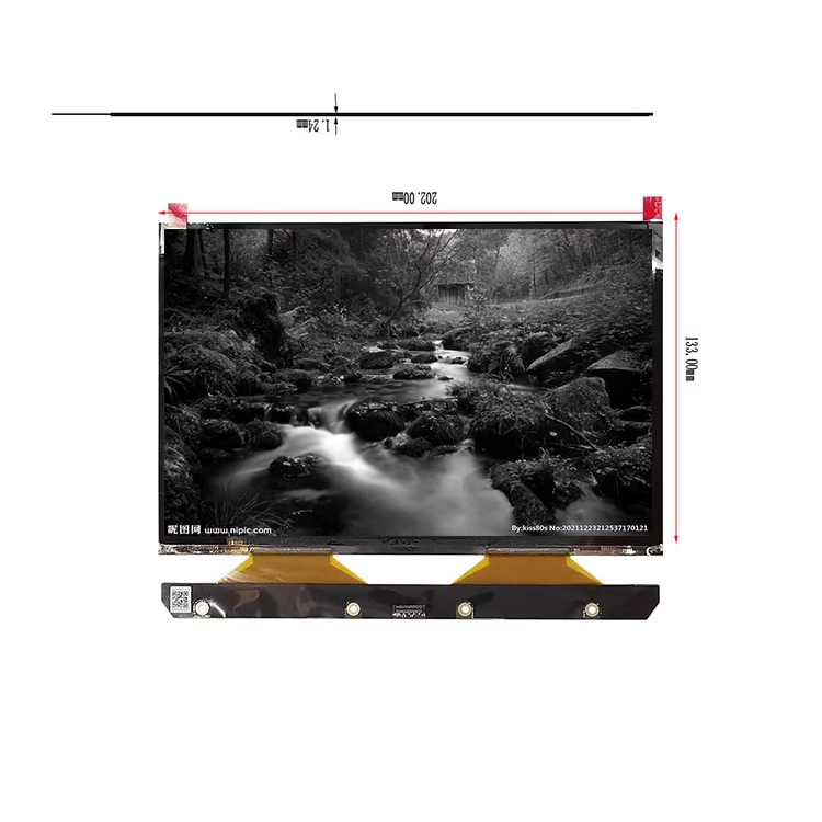
| Active area | 162.05(W) X 121.54(H) mm |
| Panel size | 183(W) X 141(H) X 3.5(D) mm |
| Surface treatme nt | Hard coating |
| Color arrangement | RGB-stripe |
| View Directi on (Gray Inversion) | IPS |
| In terface | LVDS |
| Panel power consumption | TBD (Typ ) |
| Weight | TBD |
| Module lifetime(Hours) | 50000 |
| Pin No. | Symbol | I/O | Function |
|---|---|---|---|
| 1 | VCOM | P | Common Voltage |
| 2 | VDD | P | Power Voltage for digital circuit |
| 3 | VDD | P | Power Voltage for digital circuit |
| 4 | NC | 一 | No conn ection |
| 5 | Reset | I | Global reset pin |
| 6 | STBYB | I | Standby mode, Normally pulled high STBYB = X : normal operation STBYB = “0: timing controller, source driver will turn off, all output are High-Z |
| 7 | GND | P | Ground |
| 8 | RXIN0- | I | -LVDS differential data input |
| 9 | RXIN0+ | I | + LVDS differential data input |
| 10 | GND | P | Ground |
| 11 | RXIN1- | I | ・ LVDS differential data input |
| 12 | RXIN1 + | I | + LVDS differential data input |
| 13 | GND | P | Grou nd |
| 14 | RXIN2- | I | -LVDS differential data input |
| 15 | RXIN2+ | I | + LVDS differential data input |
| 16 | GND | P | Ground |
| 17 | RXCLKIN- | I | -LVDS differential clock input |
| 18 | RXCLKIN+ | I | + LVDS differential clock input |
| 19 | GND | P | Grou nd |
| 20 | RXIN3- | I | ・ LVDS differential data input |
| 21 | RXIN3+ | I | + LVDS differential data input |
| 22 | GND | P | Ground |
| 23 | NC | 一 | No connect!on |
| 24 | NC | — | No connection |
| 25 | GND | P | Ground |
| 26 | NC | — | No conn ection |
| 27 | DIMO | 0 | Backlight CABC controller signal output |
| 28 | SELB | I | 6bit/8bit mode select |
| 29 | AVDD | P | Power for Analog Circuit |
| 30 | GND | P | Ground |
| 31 | LED- | P | LED Cathode |
| 32 | LED- | P | LED Cathode |
| 33 | UR | I | Horizontal inversion |
| 34 | U/D | I | Vertical inversion |
| 35 | VGL | P | Gate OFF Voltage |
| 36 | CABCEN1 | I | CABC H/W enable |
| 37 | CABCENO | I | CABC H/W enable |
| 38 | VGH | P | Gate ON Voltage |
| 39 | LED+ | P | LED Anode |
| 40 | LED+ | P | LED Anode |