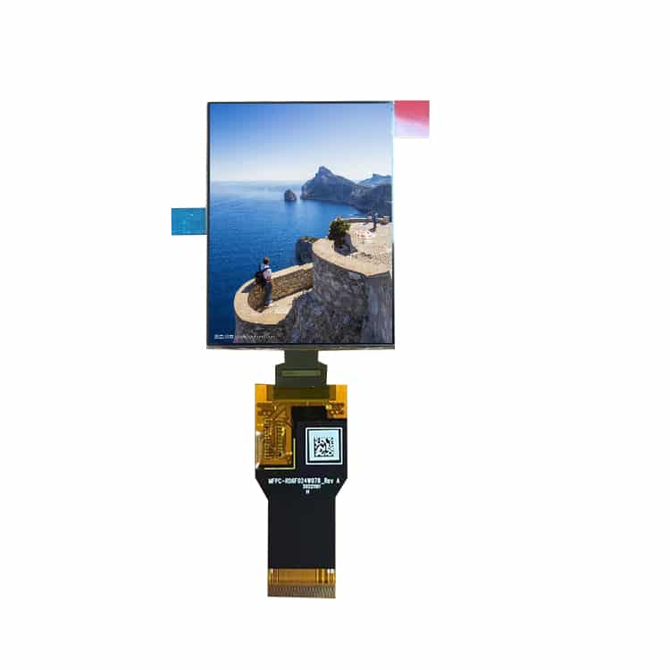
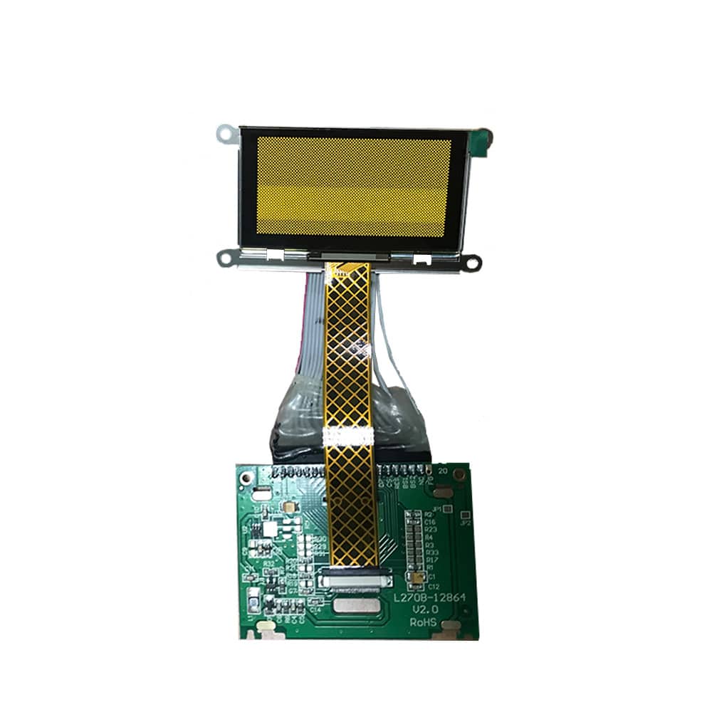
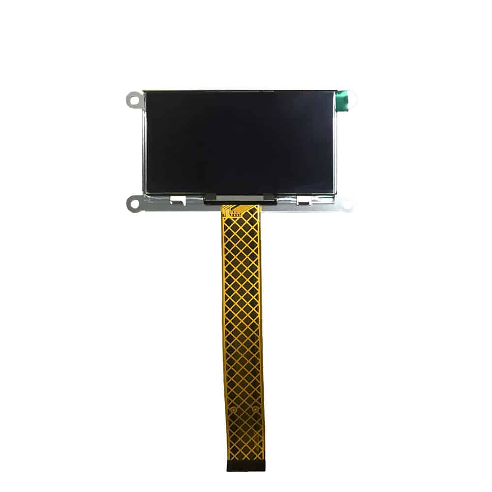
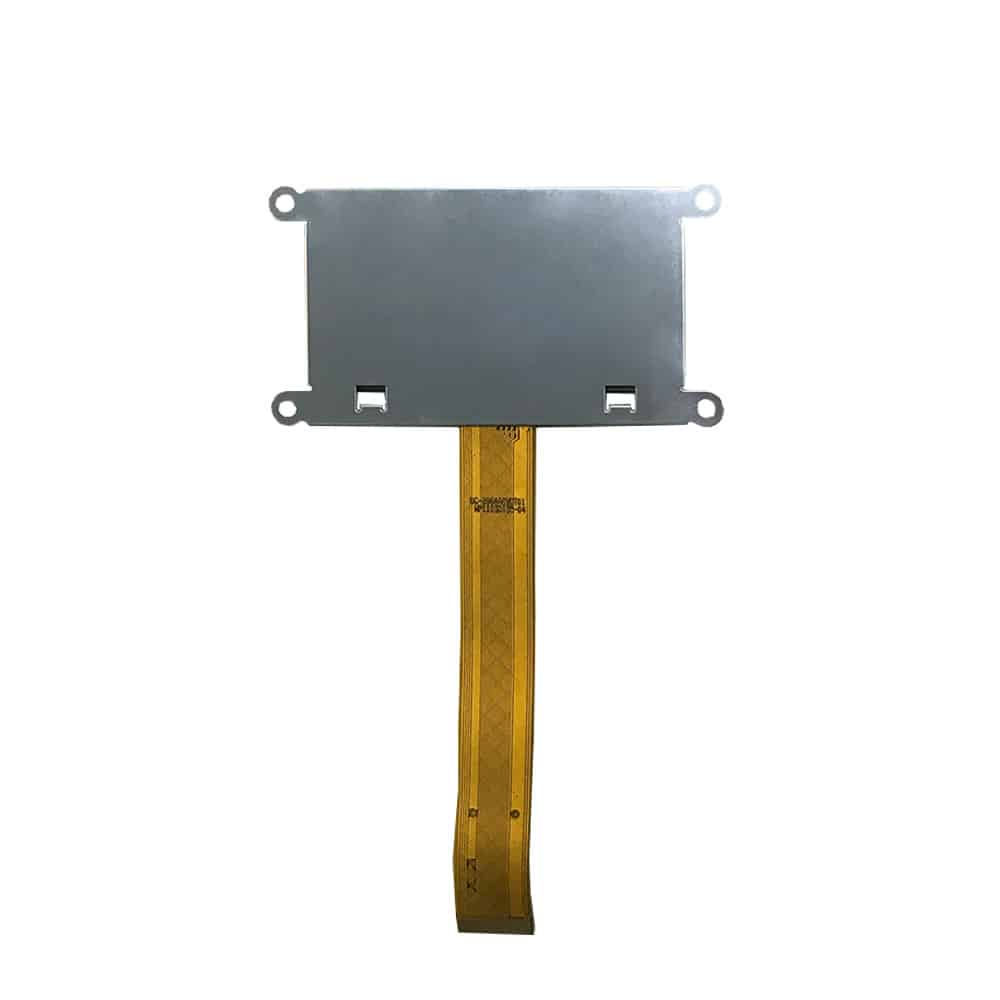
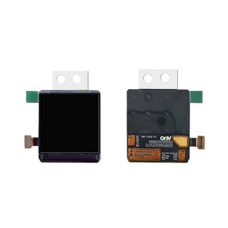
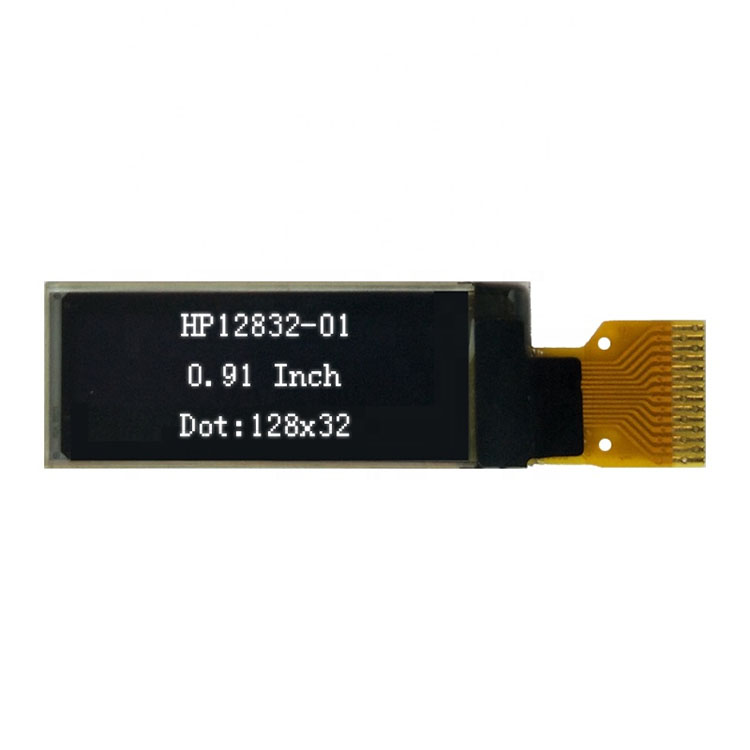
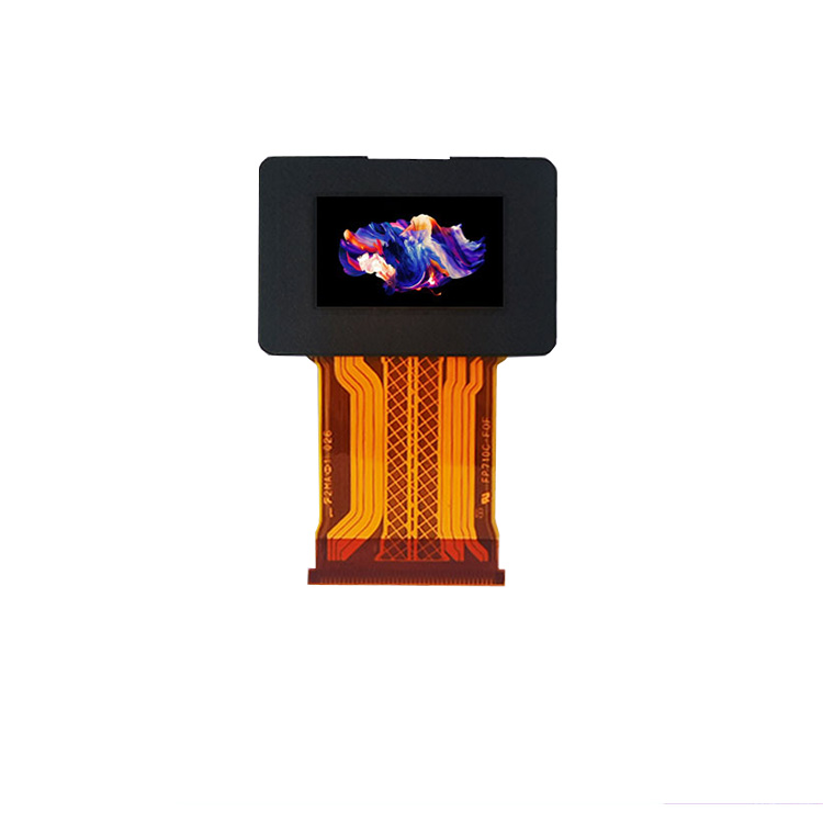
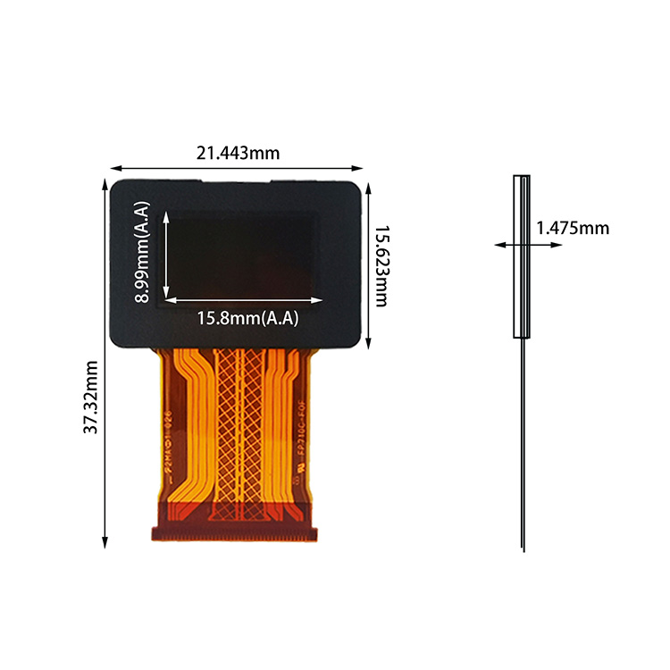
The FPC/Interface/luminance/Touch panel/Cover glass of our most products is customizable.
If you have any requirements, please contact us.
UG-2864ASYDT01 is 2.7 inch oled display screen with yellow mono color. It has Parallel/SPI interface and resolution 128*64.Driver IC is SSD1325.Outline dimension is 73.00 × 41.86 mm, thickness is 2.00 mm. Active area is 61.41 × 30.69 mm. This oled is coming out with 30 pins definition. Operating Temperature is -30~85℃, Storage Temperature is -40~90℃.
DRAWING

SPECIFICATIONS
| General Specification | |
|---|---|
| Part No. | UG-2864ASYDT01 |
| Size | 2.7 inch |
| Panel Size(mm) | 73.00 × 41.86 × 2.00 |
| Active area(mm) | 61.41 × 30.69 |
| Number of Pixel(pixels) | 128×64 |
| Operating temperature(°C) | -30 ~ 85℃ |
| Storage temperature(°C) | -40~ 90℃ |
| Driver IC | SSD1325 |
| Color | Monochrome Yellow |
| Display mode | Passive Matrix |
| Interface | 8-bit 68XX/80XX Parallel, 4-wire SPI |
| Drive Duty | 1/64 Duty |
| Weight(g) | 20.5 |
| Pins Description | |||
|---|---|---|---|
| PIN NO. | Symbol | I/O | Function |
| 1 | N.C. (GND) | - | Reserved Pin (Supporting Pin):The supporting pin can reduce the influences from stresses on the function pins. This pin must be connected to external ground. |
| 2 | VCC | P | Power Supply for OEL Panel: This is the most positive voltage supply pin of the chip. It must be supplied externally. |
| 3 | VCOMH | P | Voltage Output High Level for COM Signal: This pin is the input pin for the voltage output high level for COM signals. It can be supplied externally or internally. When VCOMH is generated internally, a capacitor should be connected between this pin and VSS. |
| 4 | IREF | I | Current Reference for Brightness Adjustment: This pin is segment current reference pin. A resistor should be connected between this pin and VSS. Set the current at 10μA. |
| 5~12 | D7~D0 | I/O | Host Data Input/Output Bus: These pins are 8-bit bi-directional data bus to be connected to the microprocessor’s data bus. When serial mode is selected, D1 will be the serial data input SDIN and D0 will be the serial clock input SCLK. |
| 13 | E/RD# | I | Read/Write Enable or Read: This pin is MCU interface input. When interfacing to a 68XX-series microprocessor, this pin will be used as the Enable (E) signal. Read/write operation is initiated when this pin is pulled high and the CS# is pulled low. When connecting to an 80XX-microprocessor, this pin receives the Read (RD#) signal. Data read operation is initiated when this pin is pulled low and CS# is pulled low. |
| 14 | R/W# | I | Read/Write Select or Write: This pin is MCU interface input. When interfacing to a 68XX-series microprocessor, this pin will be used as Read/Write (R/W#) selection input. Pull this pin to “High” for read mode and pull it to “Low” for write mode. When 80XX interface mode is selected, this pin will be the Write (WR#) input. Data write operation is initiated when this pin is pulled low and the CS# is pulled low. |
| 15 | D/C# | I | Data/Command Control: This pin is Data/Command control pin. When the pin is pulled high, the input at D7~D0 is treated as display data. When the pin is pulled low, the input at D7~D0 will be transferred to the command register. For detail relationship to MCU interface signals, please refer to the Timing Characteristics Diagrams. When the pin is pulled high and serial interface mode is selected, the data at SDIN is treated as data. When it is pulled low, the data at SDIN will be transferred to the command register. |
| 16 | RES# | I | Power Reset for Controller and Driver: This pin is reset signal input. When the pin is low, initialization of the chip is executed. |
| 17 | CS# | I | Chip Select: This pin is the chip select input. The chip is enabled for MCU communication only when CS# is pulled low. |
| 18 | N.C. | - | Reserved Pin: The N.C. pins between function pins are reserved for compatible and flexible design. |
| 19~20 | BS2,BS1 | I |  |
| 21 | VDD | P | Power Supply for Logic Circuit: This is a voltage supply pin. It must be connected to external source. |
| 22~28 | N.C. | - | Reserved Pin: The N.C. pins between function pins are reserved for compatible and flexible design. |
| 29 | VSS | P | Ground of OEL System: This is a ground pin. It also acts as a reference for the logic pins, the OEL driving voltages, and the analog circuits. It must be connected to external ground. |
| 30 | VSL | O | Voltage Output Low Level for SEG Signal: This pin is the output pin for the voltage output low level for SEG signals. A capacitor should be connected between this pin and VSS. |


