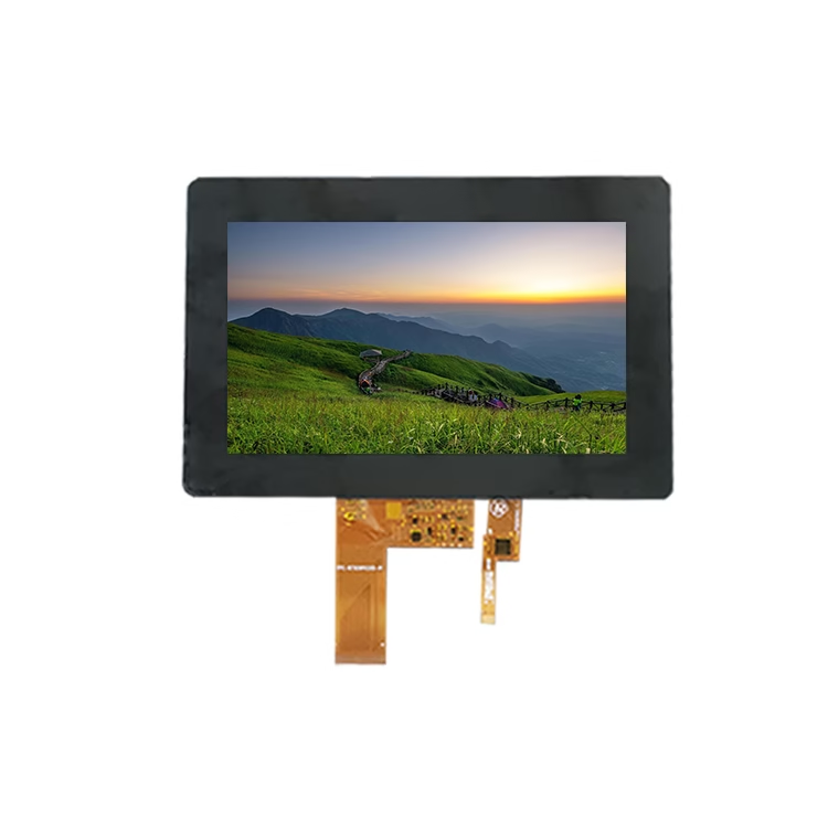
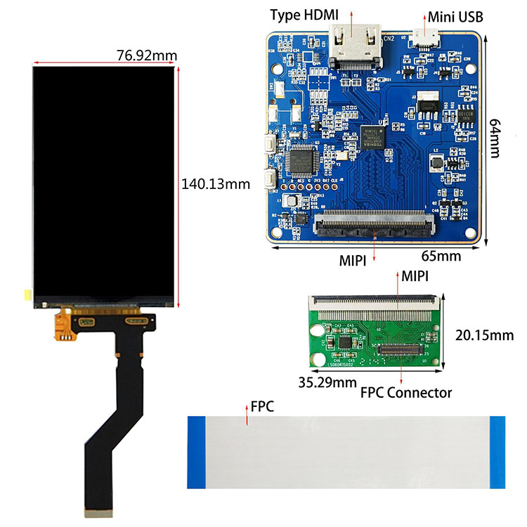
The FPC/Interface/luminance/Touch panel/Cover glass of our most products is customizable.
If you have any requirements, please contact us.
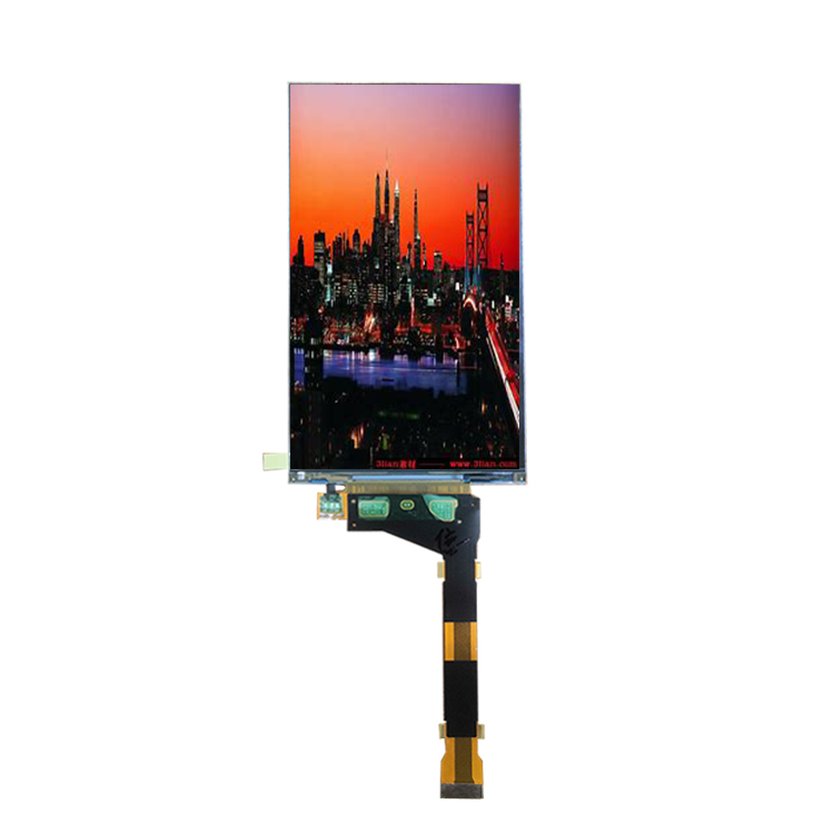
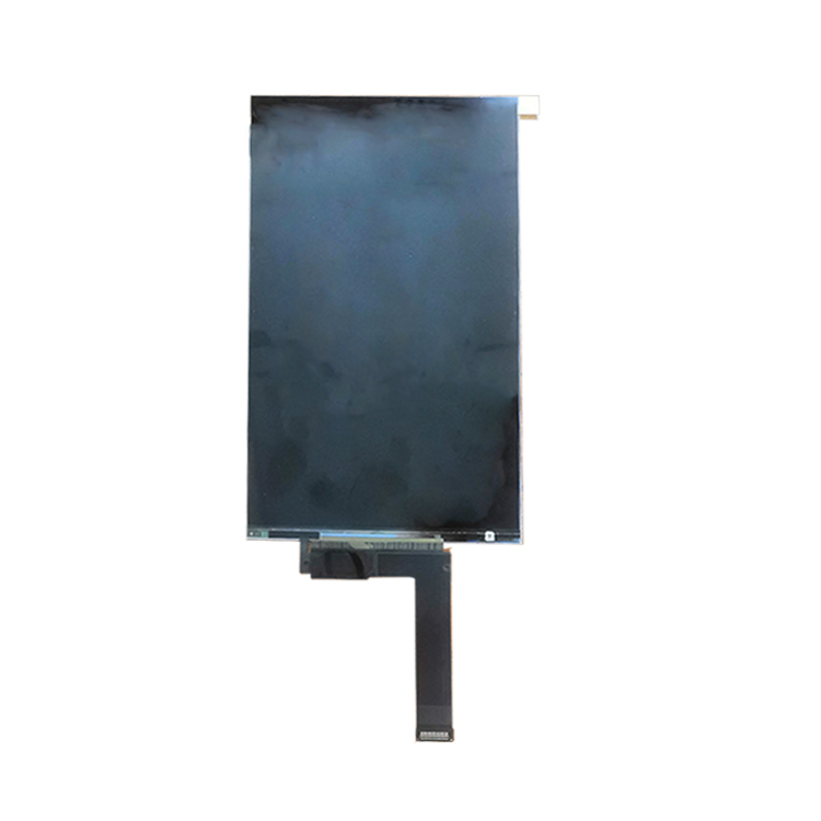
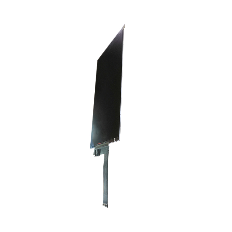
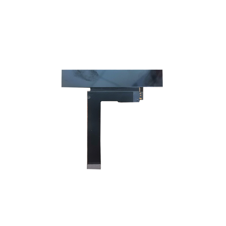
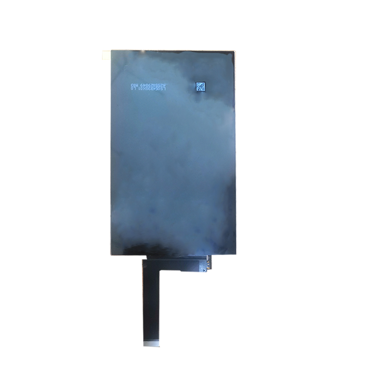
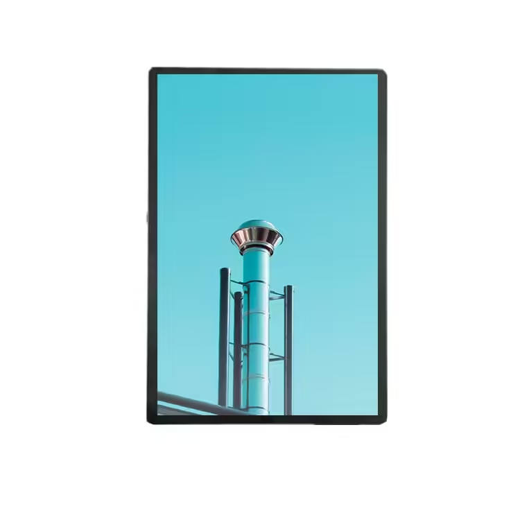
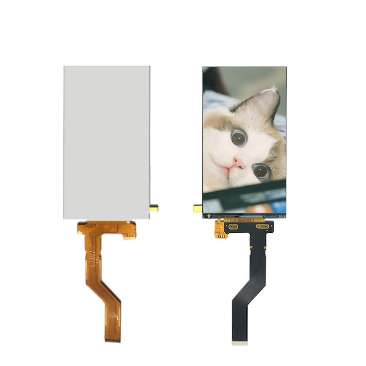
LS054B3SX01 is 5.36 inch tft lcd display module with MIPI interface and IPS All o’clock viewing angle screen. Customization is available. The shape is a rectangle with resolution 1152*1920. Outline dimension is 72.00×123.4mm, thickness is 1.27 mm. Active area is 69.984×116.64 mm. This lcd display is coming out with 32 pins definition. Working temperature is -20 to +60℃, storage temperature is -30 to +70℃.
DRAWING

SPECIFICATIONS
| General Specification | |
|---|---|
| Part No. | LS054B3SX01 |
| LCM Outline Dimension(mm) | 72.00(W)×123.4 (H)×1.27(D) |
| Active Area(mm) | 69.984(W)×116.64(H) |
| Number of Pixel(pixels) | 1152RGB(W)×1920(H) |
| Display mode | New Mode2 |
| Operating temperature(°C) | -20 ~ 60℃ |
| Storage temperature(°C) | -30 ~ 70℃ |
| Interface | MIPI |
| Driver IC | Himax HX8399A |
| LCD Mode | Transmissive |
| Pixel Pitch(mm) | 0.02025(W)×0.06075 (H) |
| Viewing Direction | All o'clock |
| Display Colors | 16.7M |
| Pins Description | ||||
|---|---|---|---|---|
| PIN NO. | Symbol | Description | I/O | Remarks |
| 1 | LED1+ | Power supply for LED(Anode) | I | |
| 2 | GND | GND level pin | - | |
| 3 | LED2+ | Power supply for LED(Anode) | I | |
| 4 | D3_N | MIPI-DSI Data differential input pins.(Data lane3) | I | |
| 5 | LED2- | Power supply forLED(Cathode) | I | |
| 6 | D3_P | MIPI-DSI Data differential input pins.(Data lane3) | I | |
| 7 | LED1- | Power supply for LED (Cathode) | I | |
| 8 | GND | GND level pin | - | |
| 9 | VGL | 3power:IC internal output signal5power: Power supply for LCD | - | 3power:For user, please open5power:VGL=-6.95±0.15V |
| 10 | D0_N | MIPI-DSI Data differential input pins.(Data lane0) | I/O | |
| 11 | GND | GND level pin | - | |
| 12 | D0_P | MIPI-DSI Data differential input pins.(Data lane0) | I/O | |
| 13 | VSP | Power supply for LCD | I | VSP=5.7±0.15V |
| 14 | GND | GND level pin | - | |
| 15 | VSN | Power supply for LCD | I | VSN=-5.7±0.15V |
| 16 | CLK_N | MIPI-DSI Clock differential input pins. | I | |
| 17 | IOVCC | Power supply for LCD | I | IOVCC=1.8±0.15V |
| 18 | CLK_P | MIPI-DSI Clock differential input pins. | I | |
| 19 | LCD_ID | Supplier information terminal (VDD level) | O | (SHARP: Connect to IOVCC) |
| 20 | GND | GND level pin | - | |
| 21 | GND | GND level pin | - | |
| 22 | DI_N | MIPI-DSI Data differential input pins.(Data lane1) | I | |
| 23 | RESET | H/W Reset pin | I | |
| 24 | D1_P | MIPI-DSI Data differential input pins.(Data lane1) | I | |
| 25 | TE | Intemal VSYNC output (use TP control) | O | |
| 26 | GND | GND level pin | - | |
| 27 | TE1 | Intemal HSYNC output (use TP control) | O | |
| 28 | D2_N | MIPI-DSI Data differential input pins.(Data lane2) | I | |
| 29 | PWM | Backlight brightness control pin | O | |
| 30 | D2_P | MIPI-DSI Data differential input pins.(Data lane2) | I | |
| 31 | VGH | 3power:IC internal output signal5power: Power supply for LCD | - | 3power:For user, please open5power:VGH=9.55±0.15V |
| 32 | GND | GND level pin | - | |


